
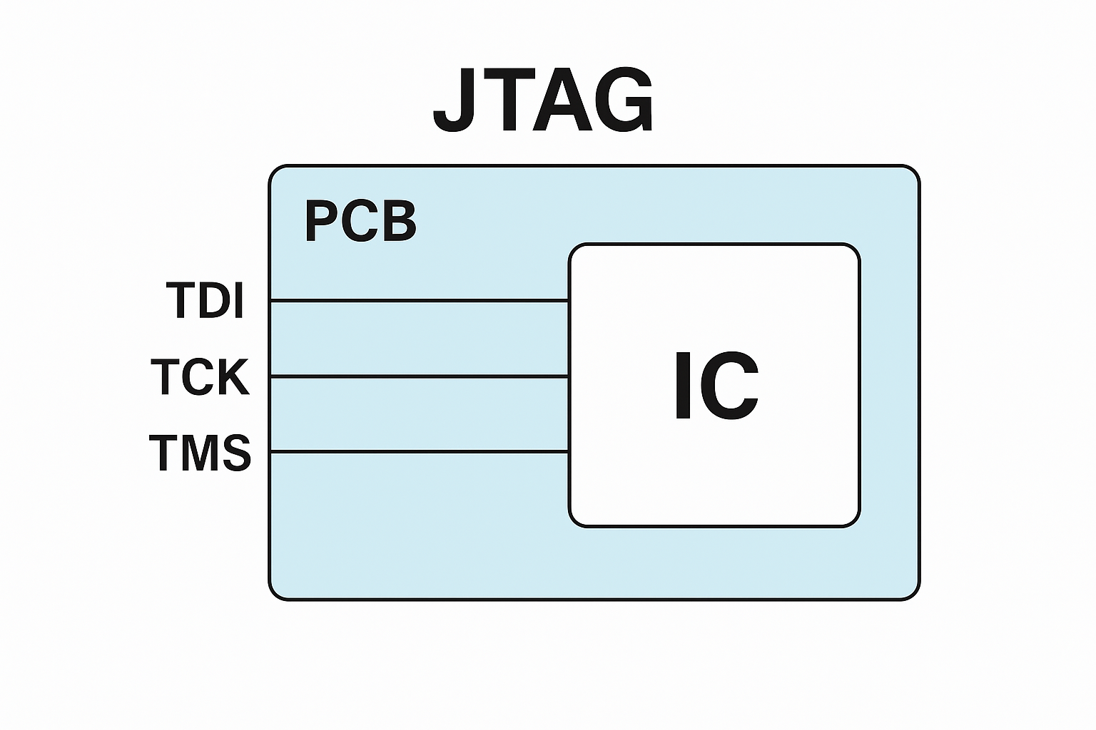
JTAG stands for Joint Test Action Group, which is the name of the group that initially developed the standard. Today, JTAG commonly refers to both the group and the test interface and protocol defined by the IEEE 1149.1 standard.
Originally created in the 1980s, JTAG was developed as a solution to a growing problem in electronics manufacturing: how to test complex circuit boards where physical access to all the pins and components was no longer possible.
Why Was JTAG Created?
As electronic components became smaller and more integrated, traditional testing methods like bed-of-nails testers or external probes couldn’t easily reach the pins or internal signals of components. JTAG was introduced to allow:
- Testing of individual pins and board connections,
- Debugging of embedded systems,
- Programming of microcontrollers, FPGAs, CPLDs, and flash memory,
- Diagnosing faults during development and manufacturing.
JTAG Is More Than Just Debugging and Programming
When most people think of JTAG, they associate it with debugging processors or programming FPGAs and CPLDs. That’s not wrong—but it’s only part of the story.
JTAG isn’t just about debugging.
It isn’t just about programming either.
While you might know JTAG through tools that connect to a JTAG interface, such as debuggers or flash programmers, those tools typically use only one part of what JTAG has to offer: the four-wire communication protocol defined by the IEEE 1149.1 standard.
What Else Can JTAG Do?
JTAG was originally developed as a solution for testing circuit boards—specifically to overcome the limitations of traditional test methods like bed-of-nails testers. These older methods required physical access to every pin or needed complex custom setups for functional testing.
To solve this, IEEE created the concept of a Test Access Port (TAP), which uses four signals (TCK, TMS, TDI, TDO) to interact with special test registers inside chips.
The key test register introduced by this standard is the Boundary Scan Register (BSR).
What Is a Boundary Scan Register?
The Boundary Scan Register sits at the edges (or “boundaries”) of a chip, between its functional logic core and the actual pins that connect it to a board. That’s why JTAG testing is often called “boundary scan” testing.
These registers are made up of individual cells that can:
- Operate in functional mode, where they don’t interfere with normal chip behavior.
- Operate in test mode, where they take control of the chip’s input/output pins.
In test mode, these boundary scan cells allow us to:
- Drive specific values onto the board’s signal lines (outputs),
- Read the values present on those lines (inputs).
How Does This Help in Testing?
Here’s the powerful part:
When JTAG is used in test mode, it allows engineers to control and observe signals on a PCB without booting the system or loading firmware. The device doesn’t need to be configured—it just needs to support boundary scan.
This means:
- You can test for short circuits, opens, and miswirings,
- You can run tests without needing full firmware or software,
- It reduces the need for physical access to test points.
Two Main Ways to Use JTAG for Testing
- Connection Testing
This basic method checks for short circuits and open connections by using only the JTAG-capable devices and their pins. It provides good coverage using the board’s layout and JTAG features. - Extended Testing (with non-JTAG devices)
Tools like XJTAG can go further by using JTAG-enabled chips to talk to non-JTAG devices (e.g., DDR RAM, Flash). This allows testing of more complex components using the existing JTAG infrastructure.
JTAG is much more than a tool for programming chips or debugging firmware. It’s a powerful hardware test interface that helps engineers:
- Test boards without physical probes,
- Check soldering and connectivity,
- Debug hardware issues early in development,
- Communicate with various components through a simple 4-pin interface.
So next time you hear “JTAG,” remember:
It’s not just a port—it’s a gateway to deep-level access and testing.
💛 Support Embedded Prep
If you find our tutorials helpful and want to support our mission of sharing high-quality embedded system knowledge, you can contribute by buying us a coffee. Every small contribution helps us keep creating valuable content for learners like you. ☕
Thank you for your support — it truly keeps Embedded Prep growing. 💻✨
1. Introduction
When working with embedded systems, hardware debugging, or board-level testing, JTAG is a name that comes up often. But what exactly is it?
JTAG stands for Joint Test Action Group—the name of the group that developed the standard. It’s an interface and protocol that allows you to test, debug, and program devices on a circuit board, even when they are soldered down and inaccessible through traditional means.
2. What is JTAG?
At its core, JTAG is a standard for verifying designs and testing printed circuit boards (PCBs) after manufacture. It provides a standardized interface to communicate with chips using just a few pins.
JTAG was standardized as IEEE 1149.1 in 1990 and is commonly used in embedded systems, FPGA programming, microcontroller debugging, and boundary scan testing.
3. Why Was JTAG Introduced?
Before JTAG, engineers used bed-of-nails testers or manually probed signals on PCBs. These methods had major drawbacks:
- Couldn’t access densely packed surface-mount devices (SMDs)
- Fragile and expensive test fixtures
- Not scalable for complex boards
JTAG solved this by embedding test logic inside chips, allowing for internal signal monitoring and control through a serial interface—no need to physically touch internal nodes!
4. How Does JTAG Work?
JTAG enables access to a device’s internal functions using a serial protocol and a Test Access Port (TAP). This port can:
- Control internal registers
- Access memory
- Perform boundary scans
- Program flash memory
The TAP connects to a chain of devices called a JTAG daisy chain. Devices in the chain share the same control signals, but each has its own data path.
The core components inside a JTAG-enabled device include:
- TAP Controller – Controls the JTAG state machine
- Instruction Register (IR) – Decides what operation to perform (e.g., read ID, boundary scan)
- Data Registers (DR) – Used to shift in/out data
5. JTAG Pinout and Signals
JTAG usually uses 4 or 5 pins:
| Pin Name | Full Form | Description |
|---|---|---|
| TDI | Test Data In | Serial data input into the JTAG chain |
| TDO | Test Data Out | Serial data output from the JTAG chain |
| TCK | Test Clock | Provides the clock for synchronizing data |
| TMS | Test Mode Select | Controls the state of the TAP controller |
| TRST | Test Reset (optional) | Resets the JTAG state machine (not always used) |
6. Common Use Cases of JTAG
- Boundary Scan Testing
- Check connectivity between pins and trace faults without physical probing.
- In-System Programming (ISP)
- Program flash memory, FPGAs, CPLDs, and MCUs via JTAG.
- Debugging Embedded Systems
- Set breakpoints, inspect registers, view memory, and single-step through code.
- Hardware Bring-Up
- Access low-level hardware registers before firmware is ready.
7. JTAG in Embedded Systems
JTAG is essential for developers working on ARM Cortex, STM32, ESP32, or custom SoCs. It allows you to:
- Flash firmware without bootloader
- Debug without printf()
- Perform post-silicon validation
Example: JTAG with STM32
Using an ST-Link or J-Link programmer, you can connect to the STM32 via JTAG or SWD (Serial Wire Debug, a 2-wire variant) and debug using tools like OpenOCD + GDB or STM32CubeIDE.
8. Tools and Software for JTAG
Hardware Debug Probes:
- SEGGER J-Link
- ST-Link (for STM32)
- TI XDS110 (for TI MCUs)
- FTDI-based cables (DIY options)
Software:
- OpenOCD (Open On-Chip Debugger) – Popular open-source JTAG interface
- GDB – GNU debugger for step-through debugging
- Vendor IDEs – STM32CubeIDE, IAR, Keil MDK, Code Composer Studio
9. Advantages and Limitations
Advantages
- Access internal registers and memory
- Non-intrusive testing and debugging
- Programming without bootloader
- Works even when the system is not fully booted
Limitations
- Not supported by all chips
- Configuration can be complex for beginners
- Risk of bricking if improperly used
- JTAG interfaces can be disabled for security in some products
10. Conclusion
JTAG is a powerful and essential interface for hardware debugging, device testing, and embedded system development. While it may seem complex at first, learning JTAG opens the door to low-level system access, deep debugging, and smoother hardware bring-up processes.
If you’re working with microcontrollers, FPGAs, or custom PCBs, understanding JTAG is a must-have skill.
FAQ – Master JTAG (Joint Test Action Group): A Beginner-Friendly, In-Depth Guide (2025)
1. What is JTAG and why should I learn it?
JTAG (Joint Test Action Group) is a standard (IEEE 1149.1) used for testing, programming, and debugging hardware—mainly microcontrollers, FPGAs, and CPUs. Learning JTAG is essential for embedded developers, hardware engineers, and system testers as it gives direct access to chip internals, enabling tasks like:
- Boundary-scan testing (fault detection on PCBs)
- Flashing firmware directly
- Debugging software running on target boards
2. What are the typical use cases of JTAG?
- Hardware testing: Identify faulty components or soldering defects.
- Firmware flashing: Load firmware into non-volatile memory without a bootloader.
- Real-time debugging: Step through code, inspect registers, memory, and control execution.
- Board bring-up: Debug and validate hardware during prototype development.
3. Which hardware tools do I need for JTAG?
You typically need:
- A JTAG debugger/programmer (e.g., SEGGER J-Link, ST-LINK, OpenOCD-compatible dongles)
- A target device that supports JTAG (e.g., STM32, ARM Cortex-M, Xilinx FPGAs)
- A JTAG connector (e.g., 10-pin, 20-pin headers)
- JTAG-compatible software tools (OpenOCD, GDB, manufacturer-specific IDEs)
4. What are the standard JTAG pinouts and signals?
Typical JTAG signals include:
- TDI (Test Data In) – Data input to the target
- TDO (Test Data Out) – Data output from the target
- TCK (Test Clock) – Clock signal
- TMS (Test Mode Select) – Controls state transitions
- TRST (optional) – Test Reset
- GND – Ground
- Vref – Reference voltage (for logic level compatibility)
5. How does JTAG work internally?
JTAG uses a TAP controller (Test Access Port), which moves through states based on the TMS and TCK lines. It shifts data into registers (e.g., instruction register, data register) and enables control over internal signals without requiring CPU code execution.
6. Is JTAG only for testing hardware?
No. While JTAG was initially designed for boundary-scan testing, it evolved to support:
- Flash programming
- Low-level debugging
- Chip-level introspection
- Reset and boot control
7. Can I use JTAG with open-source tools?
Yes. Tools like:
- OpenOCD (Open On-Chip Debugger) for programming and debugging
- GDB for source-level debugging with breakpoints and watchpoints
- UrJTAG for boundary-scan and low-level testing
These tools are often free and widely supported.
8. What’s the difference between JTAG and SWD (Serial Wire Debug)?
- JTAG: 4–5 signals; full IEEE 1149.1 standard; widely supported.
- SWD: ARM-specific 2-wire protocol; lighter and faster; used on Cortex-M devices.
Both support debugging and programming, but SWD is preferred for space-constrained designs.
9. What are boundary-scan and chain configurations in JTAG?
Boundary-scan: Allows testing of I/O pins without booting the processor.
JTAG chain: Multiple devices can be connected in series (TDI → TDO) using a single JTAG interface. Each device has a unique ID and is accessed through a specific instruction.
10. What are common JTAG errors and how do I fix them?
| Error | Cause | Fix |
|---|---|---|
| Target not found | Wrong pinout, bad solder | Check wiring, use multimeter |
| Device ID mismatch | Wrong chip selected | Check chain or update config |
| No response to TCK/TMS | Dead chip or damaged port | Try alternate device or port |
| OpenOCD config failed | Wrong interface/chip | Double-check .cfg files |
11. Can JTAG be used on production devices?
Yes, but JTAG is often disabled or locked for security reasons in production devices. Secure provisioning may require unlocking or access keys.
12. Where can I practice JTAG debugging hands-on?
Start with:
- STM32 Nucleo or Discovery boards
- ESP32 DevKit
- Raspberry Pi with GPIO for JTAG
- FPGAs like Xilinx or Intel (with USB Blaster, Platform Cable)
Use OpenOCD + GDB or manufacturer IDEs (STM32CubeIDE, Xilinx Vivado, etc.).
13. What are the career benefits of learning JTAG?
Mastering JTAG gives you an edge in:
- Embedded software development
- Board-level diagnostics
- Hardware testing and verification
- Secure firmware deployment
It’s a key skill for Embedded Engineers, Firmware Developers, and Test Engineers.
You can also Visit other tutorials of Embedded Prep
- What is eMMC (Embedded MultiMediaCard) memory ?
- Top 30+ I2C Interview Questions
- Bit Manipulation Interview Questions
- Structure and Union in c
- Little Endian vs. Big Endian: A Complete Guide
- Merge sort algorithm
Special thanks to @mr-raj for contributing to this article on EmbeddedPrep
Mr. Raj Kumar is a highly experienced Technical Content Engineer with 7 years of dedicated expertise in the intricate field of embedded systems. At Embedded Prep, Raj is at the forefront of creating and curating high-quality technical content designed to educate and empower aspiring and seasoned professionals in the embedded domain.
Throughout his career, Raj has honed a unique skill set that bridges the gap between deep technical understanding and effective communication. His work encompasses a wide range of educational materials, including in-depth tutorials, practical guides, course modules, and insightful articles focused on embedded hardware and software solutions. He possesses a strong grasp of embedded architectures, microcontrollers, real-time operating systems (RTOS), firmware development, and various communication protocols relevant to the embedded industry.
Raj is adept at collaborating closely with subject matter experts, engineers, and instructional designers to ensure the accuracy, completeness, and pedagogical effectiveness of the content. His meticulous attention to detail and commitment to clarity are instrumental in transforming complex embedded concepts into easily digestible and engaging learning experiences. At Embedded Prep, he plays a crucial role in building a robust knowledge base that helps learners master the complexities of embedded technologies.


It’s very straightforward to find out any matter on net as compared to
textbooks, as I found this piece of writing at this website.