Author: admin

  • Master ARM Cortex-M Exception Handling (2026)

    What is Exception Handling in ARM Cortex-M?

    ARM Cortex-M Exception Handling: In ARM Cortex-M, exceptions are interrupts and system events that cause the processor to temporarily stop the main program and execute a special function (handler) to deal with it.

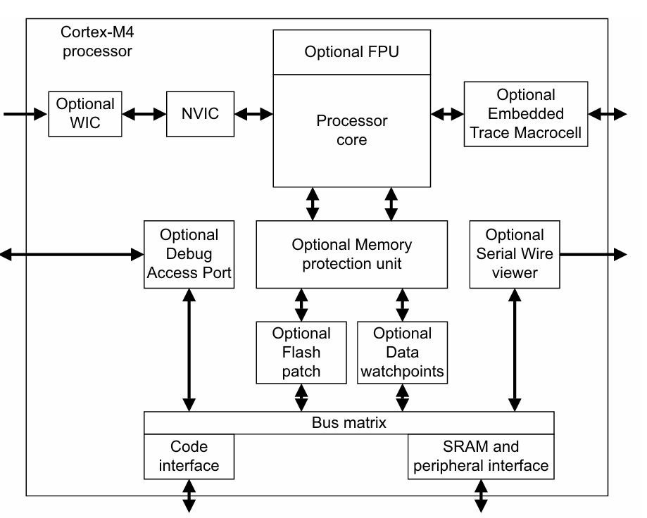
    ✅ Cortex-M CPUs have a built-in Nested Vectored Interrupt Controller (NVIC) that supports exceptions, prioritization, nesting, and vector table.

    Types of Exceptions

    CategoryExamplesTriggered By
    System ExceptionsReset, NMI, HardFault, SysTick, PendSV, etc.System events or faults
    Fault ExceptionsMemManage, BusFault, UsageFaultErrors in code or hardware
    External Interrupts (IRQs)Timer, GPIO, UART, etc.Peripheral hardware requests

    What is an Exception?

    An exception is a special event that interrupts the normal program execution and transfers control to a special function called an exception handler.

    You can think of it like this:

    “Hey CPU, stop what you’re doing. Something important just happened. Handle it now!”

    Types of Exceptions in Cortex-M4

    The ARM Cortex-M4 processor has two main types of exceptions:

    TypeDescription
    Interrupts (IRQs)Triggered by external devices like timers, buttons, UART, etc.
    System ExceptionsTriggered internally by the processor (like faults, system calls, etc.)

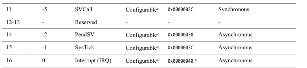
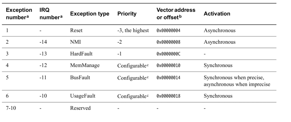
    List of System Exceptions (with vector numbers)

    Here are some common system exceptions:

    Exception NameVector NumberDescription
    Reset1Happens when the processor starts or is reset.
    NMI (Non-Maskable Interrupt)2A high-priority interrupt that cannot be disabled.
    HardFault3Happens when something goes seriously wrong (e.g., invalid memory access).
    MemManage Fault4Memory protection violation.
    BusFault5Bus error during instruction/data access.
    UsageFault6Illegal instructions (like divide by zero, etc).
    SVCall11Supervisor Call (used in RTOS or OS).
    PendSV14Used in context switching in RTOS.
    SysTick15Timer interrupt, often used for OS ticks.

    What Happens When an Exception Occurs?

    1. Processor saves context (automatically):
      • Saves registers: R0-R3, R12, LR, PC, xPSR onto the stack.
    2. Jumps to the exception handler:
      • The address is taken from the vector table.
    3. Executes handler function.
    4. Returns to where it was using BX LR or exception return sequence.

    Vector Table

    The vector table is a list of addresses stored at the beginning of memory (0x00000000). Each entry is a pointer to the handler for each exception.

    Example:

    void (* const vector_table[])() __attribute__((section(".isr_vector"))) = {
        (void*) 0x20002000,   // Initial Stack Pointer
        Reset_Handler,        // Reset
        NMI_Handler,          // NMI
        HardFault_Handler,    // HardFault
        ...
    };

    Common Fault Exceptions

    1. HardFault

    • Most serious.
    • Happens when no other fault handler catches the error.
    • Example: Dereferencing a NULL pointer.

    2. MemManage Fault

    • Related to memory protection (MPU).
    • Example: Accessing restricted memory.

    3. BusFault

    • Caused by bus errors during instruction fetch or data access.
    • Example: Accessing non-existent memory address.

    4. UsageFault

    • Caused by incorrect use of instructions.
    • Example: Division by zero, unaligned access.

    How to Write a Simple Exception Handler

    Example for HardFault:

    void HardFault_Handler(void) {
        while (1) {
            // Stay here forever - you can add logging or LED blink
        }
    }
    

    SysTick and PendSV (RTOS Related)

    • SysTick: Regular timer interrupt (e.g., every 1ms) used to keep track of time.
    • PendSV: Used for context switching in operating systems.

    These are critical for implementing real-time operating systems.

    Registers Involved

    • xPSR (Program Status Register): Gives status of current program state.
    • LR (Link Register): Helps in return from exception.
    • PC (Program Counter): Address of the instruction being executed.

    Debugging Tips

    • Check the value of the LR (Link Register) to know where the exception came from.
    • You can decode the value of LR to understand the exception return type (called EXC_RETURN).

    Exception Types in Cortex-M4 (Made Simple)

    1. Reset

    • What is it?
      It happens when you first turn on the microcontroller (power-up) or when it’s manually reset (like pressing a reset button).
    • What does it do?
      The processor starts from the beginning — it looks at a specific address (in the vector table) and starts running your main code.
    • Think of it like:
      Turning off and on your computer — it restarts from scratch.

    2. NMI (Non-Maskable Interrupt)

    • What is it?
      It’s a very important interrupt that cannot be ignored or turned off.
    • When does it happen?
      Triggered by special hardware problems or important peripherals.
    • Why is it special?
      • It can’t be blocked by other interrupts.
      • Only the Reset has a higher priority than NMI.
    • Think of it like:
      A fire alarm — it will ring no matter what else is going on.

    3. HardFault

    • What is it?
      A major error that happens when something really bad occurs — like accessing invalid memory or when another exception fails.
    • When does it happen?
      • Program tries to use a bad address.
      • An exception cannot be handled properly.
    • What makes it special?
      • Has very high priority (second only to Reset and NMI).
      • Can’t be ignored if it happens.
    • Think of it like:
      A system crash or blue screen. The processor doesn’t know what to do and enters a special error state.

    4. MemManage Fault

    • What is it?
      A memory access error — trying to read or write to protected or forbidden areas in memory.
    • Example:
      Trying to execute code in a non-executable area.
    • Think of it like:
      You tried opening a locked door. You’re not allowed in.

    5. BusFault

    • What is it?
      Happens when something goes wrong while moving data to or from memory (like over a bus).
    • Example:
      You try to read from a memory location that doesn’t respond or doesn’t exist.
    • Think of it like:
      A delivery truck goes to an address, but no one is there to accept the package.

    6. UsageFault

    • What is it?
      Happens when you use instructions incorrectly.
    • Examples:
      • Using an undefined instruction
      • Dividing by zero
      • Using misaligned memory access
    • Think of it like:
      Typing a wrong command in a computer program — something the processor doesn’t understand.

    7. SVCall (Supervisor Call)

    • What is it?
      It’s triggered by a special instruction in the program (called SVC).
    • Why is it used?
      To ask the operating system for help — like calling a system function or driver.
    • Think of it like:
      A customer service call — your code is asking the OS for assistance.

    8. PendSV (Pending Supervisor Call)

    • What is it?
      A special interrupt used for context switching in an operating system.
    • When is it used?
      When the OS wants to switch from one task to another.
    • Think of it like:
      Switching between open apps on your phone — only when the current one is done.

    9. SysTick

    • What is it?
      A system timer interrupt that goes off at regular time intervals (like every 1 millisecond).
    • Why is it useful?
      • Used by RTOS (real-time operating systems) to keep track of time.
      • Helps schedule tasks.
    • Think of it like:
      A ticking clock that reminds the CPU to check tasks.

    10. Interrupt (IRQ)

    • What is it?
      Regular interrupts triggered by external devices like:
      • Timers
      • Buttons
      • Sensors
    • Why are they important?
      Peripherals use IRQs to alert the processor when they need attention.
    • Think of it like:
      Your phone buzzing — something needs your attention.

    Summary Table

    Exception TypeSimple MeaningWho Triggers ItCan It Be Turned Off?
    ResetSystem restartPower or reset buttonNo
    NMIEmergency interruptHardwareNo
    HardFaultSerious errorProcessorNo
    MemManageBad memory accessProcessorYes
    BusFaultMemory bus errorProcessorYes
    UsageFaultWrong instructionProcessorYes
    SVCallSystem service requestSoftwareYes
    PendSVTask switch requestSoftware/OSYes
    SysTickTimer interruptTimerYes
    IRQNormal interruptPeripheralsYes

    Final Notes

    • Exceptions help the processor react to important or error conditions.
    • Some are triggered by hardware (like Reset, NMI), some by your own code (like SVCall).
    • Faults like HardFault, UsageFault help catch bugs and protect your system.
    What Are Exception States?

    When an exception (like an interrupt or a fault) occurs, the processor doesn’t just instantly handle it — instead, that exception goes through different states.

    Think of it like a queue at a doctor’s clinic:

    • You wait your turn (Pending)
    • You go inside to be treated (Active)
    • You’re done and leave (Inactive)
    • And sometimes, you’re inside while someone else knocks — that’s Active and Pending!

    The 4 States of an Exception

    1. Inactive

    • What it means:
      Nothing is happening — the exception is not triggered or being serviced.
    • Example:
      No interrupt from a button press or sensor — the CPU is doing regular work.

    2. Pending

    • What it means:
      The exception is waiting to be handled by the processor.
    • How it gets here:
      • A peripheral device (like a timer or sensor) sends an interrupt.
      • Software writes to a register to generate an interrupt.
    • Example:
      You press a button → that sends an interrupt → the exception becomes pending, waiting for the CPU to respond.

    3. Active

    • What it means:
      The CPU is currently handling the exception — it’s running the exception handler code.
    • Example:
      The CPU stops what it was doing and jumps to the interrupt handler for your button press.

    4. Active and Pending

    • What it means:
      The CPU is already handling this exception, and another one just came in from the same source — so now it’s both active and pending.
    • Important Note:
      • The CPU won’t handle the new request until the current one finishes.
      • This can happen if, for example, a timer interrupt happens again while the CPU is still handling the previous one.

    Key Notes (Simplified)

    🔁 Can one exception interrupt another?

    Yes! If a higher priority exception occurs while a lower priority one is being handled, it can interrupt it.
    Then both are in Active state, but the higher one is being serviced.

    Table Summary

    StateWhat it means
    InactiveNothing is happening. Not triggered or running.
    PendingWaiting in line. Triggered but not yet handled.
    ActiveCPU is handling it right now.
    Active & PendingCPU is still handling it, but another trigger from the same source just came.

    Real-World Analogy

    Imagine you’re a doctor (CPU) at a clinic:

    • Inactive: No patients in the waiting room.
    • Pending: A patient arrives and takes a seat in the waiting room.
    • Active: You’re currently treating a patient.
    • Active & Pending: While treating a patient, the same patient sends a new report (like a new symptom appears) — you’ll check that next.

    What is the System Control Block (SCB)?

    The System Control Block (SCB) is a special part of the ARM Cortex-M microcontroller that helps the system control and manage important operations, especially related to exceptions and faults (like errors or interrupts).

    Think of SCB as the “Control Room” of the system

    Just like a control room in a building handles alarms, system messages, and settings, the SCB handles things like:

    • Configuration settings
    • Control of system behavior
    • Reports on errors and exceptions

    What exactly does SCB do?

    1. Stores Information:
      • It contains information about how the system is set up.
      • For example, it knows what kind of CPU core you’re using and other system details.
    2. Controls Exceptions:
      • Exceptions are special events like:
        • An interrupt from a timer
        • A fault caused by invalid memory access
      • SCB helps control how the system responds to these events.
    3. Helps in Debugging:
      • It can report errors or faults that occur, which helps you debug your code.

    Where is it used?

    • It’s part of the core of ARM Cortex-M processors.
    • Used when handling:
      • Fault exceptions like hard faults or memory faults
      • System resets
      • Vector table settings (which tell the system what to do when something happens)

    Registers in SCB (just names for now):

    Here are some important registers inside the SCB (you don’t have to memorize them yet):

    • CPUID: Tells which processor you’re using
    • ICSR: Controls system exceptions
    • AIRCR: Lets you request a system reset
    • SCR: Controls system sleep modes
    • CCR: Enables/disables certain features like fault trapping
    • SHCSR: Shows which exceptions are enabled or active

    In Short:

    The SCB is a built-in control unit in ARM Cortex-M processors that manages exceptions, faults, and system control features like resets and sleep modes. It’s like the system’s supervisor.

    System Control Block (SCB) registers are part of the Cortex-M System Control Space, which provides system-level configuration and control features like interrupt priority, fault handling, system reset, and debug support.

    Here’s a breakdown of each column:

    Columns

    ColumnMeaning
    AddressThe memory-mapped address of the register in the SCB address space.
    NameName of the register.
    TypeRead/Write access: RW (Read/Write), RO (Read-Only), etc.
    Required PrivilegeOnly privileged code (like kernel or supervisor mode) can access it.
    Reset ValueThe value stored in the register after reset.
    DescriptionFunction of the register.

    Important Registers Explained

    RegisterAddressPurpose
    ACTLR0xE000E008Auxiliary Control Register – Enables/Disables implementation-specific features.
    CPUID0xE000ED00CPUID Base Register – Read-only; identifies the processor type and revision.
    ICSR0xE000ED04Interrupt Control and State Register – Controls pending interrupts and tracks the current interrupt number.
    VTOR0xE000ED08Vector Table Offset Register – Points to the interrupt vector table in memory.
    AIRCR0xE000ED0CApplication Interrupt and Reset Control Register – Software reset, endianness config, interrupt priority grouping.
    SCR0xE000ED10System Control Register – Configures deep sleep, sleep-on-exit, etc.
    CCR0xE000ED14Configuration and Control Register – Enables stack alignment, fault traps, etc.
    SHPRx0xE000ED18 to 0xE000ED20System Handler Priority Registers – Set priorities for system exceptions like SVCall, PendSV, SysTick.
    SHCSR0xE000ED24System Handler Control and State Register – Enables system exceptions and indicates their active/pending states.
    CFSR0xE000ED28Configurable Fault Status Register – Reports details of usage, bus, or memory faults.
    MMSR/BFSR/UFSR(parts of CFSR)Subfields of the CFSR to provide more specific fault information.
    HFSR0xE000ED2CHardFault Status Register – Indicates causes of HardFault exceptions.
    MMAR0xE000ED34MemManage Fault Address Register – Address that caused memory fault.
    BFAR0xE000ED38BusFault Address Register – Address that caused bus fault.
    AFSR0xE000ED3CAuxiliary Fault Status Register – Optional register for vendor-specific fault status.

    Key Concepts

    • Privileged Access: These registers can only be modified in privileged mode, ensuring the kernel has control over critical system behavior.
    • Reset Values: These default values indicate the state of the register after a system reset.
    • Exception Handling: Many of these registers are used for handling and prioritizing faults/exceptions.
    Enable PendSV and fault exceptions (Memory Management, BusFault, UsageFault) on an ARM Cortex-M processor, you’ll work with specific SCB system control registers. These are:

    1. Enabling PendSV Exception

    PendSV (Pendable Service Call) is enabled by default, but you may need to:

    • Set its priority to control preemption.
    • Pend it manually using ICSR.

    ✅ Set PendSV Priority (lowest)

    #define SCB_SHPR3    (*(volatile uint32_t *)0xE000ED20)
    #define PENDSV_PRIO_POS  16  // Bits 23:16 are for PendSV priority
    
    void enable_pendsv_lowest_priority(void) {
        // Set PendSV to lowest priority (0xFF)
        SCB_SHPR3 |= (0xFF << PENDSV_PRIO_POS);
    }
    

    ✅ Manually Pend the PendSV exception

    #define SCB_ICSR     (*(volatile uint32_t *)0xE000ED04)
    #define ICSR_PENDSVSET (1 << 28)
    
    void trigger_pendsv(void) {
        SCB_ICSR |= ICSR_PENDSVSET;  // Set bit 28 to pend PendSV
    }
    

    PendSV Handler Setup

    You must implement the handler function like this:

    void PendSV_Handler(void) {
        // Your context switch or deferred processing here
    }
    

    2. Enabling Fault Exceptions

    By default, fault handlers are disabled (except HardFault). You must enable:

    • Memory Management Fault
    • BusFault
    • UsageFault

    ✅ Use SCB_SHCSR to enable faults:

    #define SCB_SHCSR     (*(volatile uint32_t *)0xE000ED24)
    
    #define MEMFAULTENA   (1 << 16)
    #define BUSFAULTENA   (1 << 17)
    #define USGFAULTENA   (1 << 18)
    
    void enable_fault_exceptions(void) {
        SCB_SHCSR |= (MEMFAULTENA | BUSFAULTENA | USGFAULTENA);
    }
    

    Fault Handler Implementations

    You must implement handlers for these faults, or the system will go into HardFault if they occur:

    void MemManage_Handler(void) {
        // Handle memory fault
    }
    
    void BusFault_Handler(void) {
        // Handle bus fault
    }
    
    void UsageFault_Handler(void) {
        // Handle undefined instruction, divide by zero, etc.
    }
    

    Summary

    ExceptionEnable BitRegisterHandler
    PendSV(default enabled)SHPR3 (priority)PendSV_Handler()
    MemManageBit 16SHCSRMemManage_Handler()
    BusFaultBit 17SHCSRBusFault_Handler()
    UsageFaultBit 18SHCSRUsageFault_Handler()

    Manual triggering and handling of an interrupt (USART3) on an ARM Cortex-M processor, typically used in STM32 microcontrollers :

    /**
      ******************************************************************************
      * @file    main.c
      * @author  Nish
      * @version V1.0
      * @brief   Custom implementation: Triggering USART3 interrupt manually.
      ******************************************************************************
    */
    
    #if !defined(__SOFT_FP__) && defined(__ARM_FP)
      #warning "FPU is not initialized, but the project is compiling for an FPU. Please initialize the FPU before use."
    #endif
    
    #include <stdint.h>
    #include <stdio.h>
    
    #define USART3_IRQNO 39
    
    int main(void)
    {
    	// Step 1: Manually set the pending bit for USART3 interrupt in NVIC ISPR1
    	uint32_t *pISPR1 = (uint32_t*)0xE000E204;
    	*pISPR1 |= (1 << (USART3_IRQNO % 32));  // Force USART3 interrupt to pending state
    
    	// Step 2: Enable USART3 interrupt in NVIC ISER1
    	uint32_t *pISER1 = (uint32_t*)0xE000E104;
    	*pISER1 |= (1 << (USART3_IRQNO % 32));  // Allow USART3 interrupt to be serviced
    
    	// Infinite loop: Wait for interrupt to occur
    	for (;;);
    }
    
    // Custom ISR for USART3 interrupt
    void USART3_IRQHandler(void)
    {
    	printf("Inside custom USART3 ISR\n");
    }
    
  • Understanding Stack Memory in ARM Cortex-M4

    Stack Memory in ARM Cortex-M4 : Stack memory is an essential part of how microcontrollers like the ARM Cortex-M4 manage temporary data, especially during function calls and interrupt handling. If you’re just starting out in embedded systems or working with ARM processors, understanding stack memory is a must.

    What is Stack Memory?

    Stack memory is a special section of the main memory (RAM) that is used to temporarily store data. This data is often short-lived and needed only during certain parts of a program, such as:

    • Function execution
    • Interrupt or exception handling
    • Saving and restoring CPU register values

    Where is stack memory stored?

    • In internal RAM or external RAM of the microcontroller.
    • Allocated at the time the program starts and managed automatically.

    How Does the Stack Work?

    Stack follows a Last-In, First-Out (LIFO) rule, which means:

    • The last data pushed (added) onto the stack will be the first to be popped (removed).

    Think of it like a stack of plates: you add one plate on top, and when you need one, you take the top one off first.

    Stack Operations: PUSH and POP

    The processor uses two main instructions to work with the stack:

    InstructionAction
    PUSHSaves (stores) data on the stack
    POPRestores (retrieves) data from the stack

    These instructions automatically modify the Stack Pointer (SP).

    What is the Stack Pointer (SP)?

    • The Stack Pointer (also called SP or R13) is a special CPU register that always points to the top of the stack.
    • When you PUSH, the stack pointer decreases (stack grows downwards).
    • When you POP, the stack pointer increases.

    Stack Grows Down

    In Cortex-M4, the stack grows from high memory to low memory.

    When Is Stack Memory Used?

    Let’s go through some common use cases:

    1. 🧠 Temporary Storage of Register Values

    When a function is called, or an interrupt occurs, the processor temporarily stores important register values (like R0–R3, LR, PC, xPSR) on the stack to preserve the program state.

    2. 📦 Temporary Storage of Local Variables

    Local variables declared inside a function (e.g., int x = 5;) are stored in stack memory. These variables are automatically cleared when the function ends.

    3. 🚨 Exception or Interrupt Context Saving

    When an interrupt or system exception occurs:

    • The processor automatically stores a context on the stack.
    • This includes general-purpose registers, the processor status register (xPSR), return address (PC), and link register (LR).
    • After the ISR (Interrupt Service Routine) ends, the stack is popped, and execution resumes as if nothing happened.

    Stack in ARM Cortex-M4: Behind the Scenes

    Main and Process Stack

    Cortex-M4 has two types of stack pointers:

    Stack PointerUsage
    MSPMain Stack Pointer – used by system/interrupts
    PSPProcess Stack Pointer – used by user-level code/tasks (in RTOS)

    By default, only MSP is used in bare-metal applications. In RTOS-based systems, PSP is used for thread execution.

    Stack Overflow: A Word of Caution

    • Stack has a fixed size (set in linker script or startup code).
    • If too much data is pushed (e.g., recursive calls, large local variables), the stack can overflow into other memory areas and cause crashes.
    • This is why it’s important to allocate enough stack space and use tools to monitor usage.

    Example: What Happens During a Function Call

    Here’s what typically happens when a function is called:

    1. Return address is saved on the stack.
    2. Local variables are allocated on the stack.
    3. Registers may be saved to preserve state.

    When the function returns:

    1. Registers are restored.
    2. Local variables are removed (stack pointer moves back).
    3. Execution continues from the saved return address.

    Summary

    FeatureDescription
    LocationInternal or external RAM
    Access StyleLast In, First Out (LIFO)
    Accessed WithPUSH/POP or LD/STR instructions
    Traced UsingStack Pointer (SP/R13)
    Stack GrowthFrom higher to lower memory addresses
    Used ForFunction calls, interrupts, local variable storage
    Stack Pointers in Cortex-M4MSP (default), PSP (used in RTOS)

    What is RAM used for in Embedded Systems?

    Imagine RAM like a shelf in your workspace. Different parts of it are used for different tasks:

    1. Global Data Area:
      • This section stores global variables and static local variables.
      • It is available throughout the entire program.
      • Think of it like a drawer where you keep important items that you’ll use again and again.
    2. Heap:
      • This area is used for dynamic memory allocation (e.g., using malloc in C).
      • The size of data here is not fixed — it grows during the program’s execution when needed.
      • Think of it like a box where you add things as you go.
    3. Stack:
      • This is used during function calls.
      • It stores temporary data like:
        • Function parameters
        • Local variables
        • Return addresses
        • Interrupt frames
      • Imagine it like a stack of books. You add a book on top when you go into a function, and remove it when the function is done.

    How Does the Stack Work in ARM Cortex Mx Processors?

    ARM Cortex Mx processors use a Full Descending (FD) stack model.

    Let’s break that down:

    • Full: The memory address it points to is already in use.
    • Descending: The stack grows downwards in memory (from higher addresses to lower addresses).

    🧠 Imagine your stack is a set of boxes on a shelf, and every time you add a new box, you place it below the last one, and it already has stuff inside.

    📌 Different Types of Stack Operation Models

    There are 4 common stack models based on how they grow and whether the top pointer points to an empty or full location:

    Stack TypeMeaning
    Full Ascending (FA)Stack grows up, and the top points to a full slot.
    Full Descending (FD)Stack grows down, and the top points to a full slot. (Used by ARM Cortex Mx)
    Empty Ascending (EA)Stack grows up, and the top points to an empty slot.
    Empty Descending (ED)Stack grows down, and the top points to an empty slot.

    📌 Summary for ARM Cortex Mx:

    • Uses Full Descending (FD) stack.
    • Stack grows from high memory to low memory.
    • Top of the stack points to a valid (already used) memory location.

    What is Stack Placement?

    When a program runs on a microcontroller (like ARM Cortex-M), memory (RAM) is divided into different parts:

    • Data section (for global/static variables),
    • Heap (for dynamically allocated memory),
    • Stack (for temporary data in functions),
    • And the unused area.

    The stack grows in a specific direction depending on how the memory is managed in the system.

    📌 Two Types of Stack Placement (as shown in the top image)

    ✅ Type 1 – Stack at the Lower Memory Side

    • Data section is placed at the bottom.
    • Heap grows upwards (towards higher memory addresses).
    • Stack grows downwards (from high to low memory addresses).
    • Stack and heap are placed opposite to each other to avoid collision.

    🧠 Think of it like:

    Heap starts from the bottom and grows up.
    Stack starts from the top and grows down.

    ✅ Type 2 – Stack at the Top (High Address Side)

    • Stack starts at the top of RAM and grows down.
    • Heap grows up from below the stack.
    • Still prevents overlap between heap and stack.

    🧠 This is common in embedded systems like ARM Cortex-Mx.

    Changing Stack Pointer (SP) to PSP in Thread Mode

    Let’s understand the bottom part of the image.

    🔹 What is SP (Stack Pointer)?

    • It’s a register that always points to the top of the current stack.

    🔹 What are PSP and MSP?

    • MSP (Main Stack Pointer): Used by default after reset and in Handler mode (interrupts, exceptions).
    • PSP (Process Stack Pointer): Used in Thread mode (normal application code), for better memory separation.

    🔄 Why Change SP to PSP?

    • To separate interrupt stack (using MSP) from application stack (using PSP).
    • Helps avoid accidental stack overflow between ISR and user code.

    🔁 Summary of SP Switching:

    ModeStack Pointer Used
    Handler Mode (interrupts)MSP
    Thread Mode (application)PSP (you can switch to it manually)

    You can switch from MSP to PSP in thread mode using a special register (CONTROL register).

    📦 Stack Region Mapping (from image):

       STACK_MSP_START
           ↓ (MSP stack grows down)
       ---------------------
           (shared stack space)
       ---------------------
           ↑ (PSP stack grows up)
       STACK_PSP_END
    

    MSP and PSP can even share the same 1KB stack memory, but they must not overlap at runtime.

    In Simple Terms:

    • Stack placement can vary, but it always grows down in ARM Cortex-M.
    • Stack and heap are placed in opposite directions to avoid clash.
    • ARM Cortex-M uses MSP by default but can switch to PSP in thread mode.
    • Separating PSP and MSP improves reliability, especially in RTOS or multitasking systems.

    Code Example: Switching from MSP to PSP

    This code assumes you are writing for a bare-metal ARM Cortex-M environment.

    #include <stdint.h>
    
    // Allocate memory for PSP (Process Stack Pointer)
    #define PSP_STACK_SIZE  0x100   // 256 bytes
    __attribute__((aligned(8))) uint8_t psp_stack[PSP_STACK_SIZE];
    
    void switch_to_psp(void) {
        // Step 1: Calculate the top address of the PSP stack
        uint32_t psp_top = (uint32_t)(psp_stack + PSP_STACK_SIZE);
    
        // Step 2: Load the PSP (R13) with this address
        __asm volatile("msr psp, %0" :: "r" (psp_top));
    
        // Step 3: Change CONTROL register to use PSP in thread mode
        // Set bit 1 of CONTROL register to 1 (use PSP), and bit 0 to 0 (Privileged mode)
        __asm volatile(
            "mov r0, #2       \n"  // CONTROL.SPSEL = 1
            "msr control, r0  \n"
            "isb              \n"  // Instruction Synchronization Barrier
        );
    }
    
    int main(void) {
        // Initially MSP is used after reset
        // Switch to PSP for thread mode
        switch_to_psp();
    
        while (1) {
            // Application code using PSP
        }
    }
    

    Explanation:

    StepWhat it Does
    psp_stackAllocates memory (256 bytes) for the process stack.
    psp_topPoints to the top of the stack (stack grows downward).
    msr psp, %0Moves the value to the PSP register.
    mov r0, #2Sets bit 1 of the CONTROL register to 1 to use PSP.
    msr control, r0Applies the new CONTROL settings.
    isbEnsures the CPU uses the new stack pointer immediately.

    Output (Expected Behavior):

    • After running switch_to_psp(), your application (thread mode) will use the PSP instead of the default MSP.
    • Interrupts and exceptions will still use MSP, which is safer and prevents corruption.

    1. Physically Two Stack Pointers

    Cortex-M processors have two separate stack pointer registers:

    • MSP (Main Stack Pointer)
    • PSP (Process Stack Pointer)

    These are hardware registers, not just variables in RAM.

    2. Main Stack Pointer (MSP)

    • Default stack pointer after reset
    • Used by:
      • Interrupt handlers (exceptions, faults)
      • System-level code
      • Thread mode if PSP is not enabled
    • MSP is automatically loaded from the first word of the vector table on reset.

    3. Process Stack Pointer (PSP)

    • Used only in thread mode
    • Useful for user-level tasks or application code
    • Typically used in RTOS-based applications to give each task its own stack

    4. Switching Between MSP and PSP

    • By default, the CPU uses MSP.
    • You can switch to PSP in Thread mode using special instructions.

    5. Changing or Accessing Stack Pointers

    • Use assembly instructions:
      • MRS — Read MSP/PSP
      • MSR — Write MSP/PSP

    Example (in ARM assembly):

    MRS R0, MSP   ; Read MSP into R0
    MRS R1, PSP   ; Read PSP into R1
    MSR MSP, R2   ; Write R2 to MSP
    

    6. Changing Stack Pointer in C Code

    • Use naked functions (no prologue/epilogue), e.g. in GCC:
    __attribute__((naked)) void switch_to_psp(uint32_t pspValue) {
        __asm volatile (
            "MSR PSP, r0       \n"  // Set PSP
            "MOV r0, #0x02     \n"
            "MSR CONTROL, r0   \n"  // Switch to PSP
            "ISB               \n"
            "BX LR             \n"
        );
    }
    

    Summary Table

    FeatureMSPPSP
    Default After Reset✅ Yes❌ No
    Used in Handler Mode✅ Yes❌ No
    Used in Thread Mode✅ Yes (by default)✅ Yes (if configured)
    Common UsageSystem/Interrupt codeApplication tasks/RTOS tasks
    Switch UsingCONTROL register (bit 1)CONTROL register (bit 1)

    AAPCS

    Imagine you’re building with LEGOs, and your friend is building another part of the same model separately. For your LEGO pieces to fit together perfectly, you both need to follow the same set of instructions, right? The Procedure Call Standard for the Arm Architecture (AAPCS) is like that set of instructions, but for computer programs running on ARM-based devices (like many smartphones and embedded systems).

    What is AAPCS and Why Do We Need It?

    In simple terms, AAPCS is a standard or a set of rules that defines how different pieces of code, called subroutines or functions, “talk” to each other.

    Think about a program as a team working on a project. One team member (a function) might need another team member (another function) to do a specific task. When the first function “calls” the second function, they need a clear agreement on how to pass information, who is responsible for what, and how to hand back the results.

    The AAPCS makes sure that functions written by different people, or even compiled by different tools, can work together seamlessly. Without it, it would be like one LEGO builder using round pegs and another using square holes – things just wouldn’t connect!

    What Does the AAPCS Define? The Contract Between Functions

    The AAPCS sets up a “contract” between the function that makes the call (the caller) and the function that gets called (the callee). This contract includes:

    1. Obligations on the Caller:
      • The caller must set things up in a specific way before the called function can start. This includes putting any necessary data (called arguments or parameters) in agreed-upon places (like specific processor “slots” called registers).
    2. Obligations on the Callee (the Called Routine):
      • If the called function needs to use certain resources that the caller was also using (like some of those processor “slots” or registers), it must save the caller’s original values before using them.
      • Before it finishes, it must restore those saved values so the caller isn’t surprised by unexpected changes.
    3. Rights of the Callee:
      • The called function has permission to use certain resources and change certain parts of the program’s state to do its job.

    A Peek into the Rules: Registers in ARM

    One of the key areas AAPCS defines is how registers are used. Registers are small, super-fast storage locations within the ARM processor.

    According to the AAPCS (as mentioned in your provided information):

    • Registers R0, R1, R2, R3: These are often used to pass arguments to a function and to return a result from a function. A function can generally modify these registers without needing to save their previous values.
    • Register R14 (LR – Link Register): This special register holds the “return address” – it tells the function where to go back to in the caller’s code once it’s finished. A function can modify this (for example, if it calls another function itself).
    • PSR (Program Status Register): This holds information about the current state of the program (like if the last calculation was zero). A function can modify this.
    • Registers R4 to R11: These are considered “callee-saved” or “preserved” registers. If a function wants to use any of these registers, it must first save their current contents (e.g., push them onto a temporary storage area called the stack). Before the function finishes and returns to the caller, it must restore these registers to their original values. This ensures that the caller’s context is not disturbed.

    Who Follows These Rules?

    When a ‘C’ compiler (a tool that translates human-readable C code into machine code for the ARM processor) generates code, it must follow the AAPCS specification. This ensures that the compiled C functions can correctly call other functions, including those that might be part of the operating system or other libraries, which also adhere to AAPCS.

    In Summary

    The AAPCS is a fundamental agreement that allows different parts of an ARM program to communicate and cooperate effectively. It defines:

    • How functions call each other.
    • How data (arguments and return values) is passed.
    • Which registers can be used freely and which must be preserved.

    By having this standard, developers can write modular code, use libraries from different sources, and be confident that everything will work together smoothly on ARM-powered devices. It’s a crucial part of the Application Binary Interface (ABI) that makes the ARM ecosystem robust and interoperable.

    Here is a cleaned-up and structured explanation of stack activities during interrupts/exceptions and stack initialization tips, especially in the context of ARM Cortex-M processors:

    Stack Activities During Interrupts and Exceptions

    When an interrupt or exception occurs in an ARM Cortex-M processor:

    What Gets Automatically Pushed to Stack

    The processor automatically saves the following registers on the current stack (usually MSP unless PSP is configured for the thread):

    • R0 – R3: Argument and temporary registers
    • R12: Intra-procedure-call scratch register
    • LR: Link register (holds the return address)
    • PC: Program counter (implicitly saved for return)
    • xPSR: Program status register

    This is done to preserve the CPU state before jumping to the interrupt handler.

    Why This is Done

    This mechanism ensures that when the handler completes and performs an exception return, all the saved registers can be restored by hardware, and the processor can resume execution exactly from where it was interrupted.

    Implication for C Handlers

    Because the registers are preserved, C functions can safely be used as interrupt handlers without needing manual assembly code for saving/restoring state.

    Stack Initialization Tips

    Proper stack configuration is essential in embedded systems to avoid hard faults, memory corruption, or unpredictable behavior.

    1. Estimate Stack Size

    • Analyze the worst-case stack usage of your application: recursive functions, deep function calls, RTOS tasks, etc.
    • Use stack usage analysis tools or test under high load.

    2. Understand the Stack Growth Model

    • Full Descending (FD) – Common in ARM (stack grows down, points to valid data)
    • Others: Full Ascending (FA), Empty Descending (ED), Empty Ascending (EA) — Know which one applies to your CPU.

    3. Choose Stack Placement

    • Decide where to place the stack:
      • At end of internal RAM (typical)
      • In external memory (SDRAM) if needed
      • Avoid placing near heap or globals unless separated by enough guard space.

    4. Two-Stage Stack Initialization

    • In systems with external SDRAM:
      • Start with stack in internal RAM
      • Initialize SDRAM in startup code or main()
      • Then switch stack pointer (MSP) to use SDRAM

    5. Vector Table and MSP Initialization

    • The first word in the vector table must contain the initial value of the Main Stack Pointer (MSP).
    • Startup code sets this up before calling main().

    6. Configure Linker Script

    • Use your linker script to:
      • Define stack start and size
      • Place symbols like _estack, _stack_size, etc.
    • The startup code reads these symbols to initialize the stack pointer.

    7. RTOS Considerations

    • RTOS kernel uses:
      • MSP for system-level tasks (e.g., ISRs, scheduler)
      • PSP (Process Stack Pointer) for user threads
    • Make sure to switch to PSP in thread mode to separate kernel and user stack.

    Summary Table

    TopicKey Point
    Registers auto-savedR0–R3, R12, LR, xPSR
    Stack for exceptionsHandled by hardware (MSP/PSP)
    Stack placementInternal RAM or SDRAM
    Vector table initializationFirst entry = Initial MSP
    Linker roleDefines stack boundaries
    RTOS stack modelMSP = kernel, PSP = user tasks

    Stack Growth

    In most embedded systems (especially ARM Cortex-M), the stack grows downward — that is, toward lower memory addresses.

    Push (Grow)

    When a function is called or data is pushed:

    • SP (Stack Pointer) is decremented.
    • New data is stored at the new lower address.

    Example:

    Suppose the stack starts at 0x20001000:

    AddressValue
    0x20001000← Initial SP
    0x20000FFCR0
    0x20000FF8R1
    0x20000FF4R2
    • Pushing 3 registers caused the SP to move from 0x20001000 to 0x20000FF4.

    Stack Shrink

    When a function returns or values are popped:

    • The SP is incremented.
    • This frees up the memory that was used.

    Pop (Shrink)

    Continuing from the example:

    AddressValue
    0x20000FF4← SP after popping

    Visual Summary

    High Address ↑
       (Empty area)
    
       |       ← stack shrinks (pops)
       ↓
    +----------+ ← Stack Top (SP)
    |   Data   |
    +----------+
    |   Data   |
    +----------+
    |   Data   |
    +----------+
       ↑
       |       ← stack grows (pushes)
    Low Address ↓
    
    • Stack grows down (toward low addresses) when pushing.
    • Stack shrinks up (toward high addresses) when popping.

    On ARM Cortex-M:

    • MSP or PSP is used depending on context (handler mode or thread mode).
    • Stack pointer is always aligned to word boundaries (4 bytes).
    • During interrupts, the CPU pushes context automatically (stack grows).
    • On return from interrupt, the CPU pops context (stack shrinks).

    Common Stack Operations in C

    Example Function Call:

    void foo() {
        int a = 5;     // local variable -> stored on stack
        bar();         // function call -> return address pushed to stack
    }
    

    What Happens in Stack:

    1. Space allocated for a
    2. Return address pushed
    3. Stack grows
    4. On function return, stack shrinks (SP adjusted back)

    Stack Overflow / Underflow

    • Overflow: Stack grows beyond its allocated space → corrupts other memory
    • Underflow: Trying to pop from an empty stack → unpredictable behavior

    Key Points

    ActionEffect on SPDirection
    PushDecrementDown
    PopIncrementUp
    Function CallPush return addr + localsStack grows
    ReturnPop return addrStack shrinks
  • Master Bus Protocols and Bus Interfaces | Beginner-Friendly Guide 2026

    What is a Bus?

    Bus Protocols and Bus Interfaces : In embedded systems and computer architecture, a bus is a communication system that transfers data between components like the CPU, memory, and peripherals.

    Imagine it like a highway for data where cars (data) travel between cities (devices).

    What is a Bus Protocol?

    A bus protocol is like traffic rules for the data highway. It defines how data is transmitted over the bus:

    • Who can speak (Master/Slave)
    • When to speak (Timing)
    • How to speak (Data format)
    • Error checking, acknowledgments, etc.

    What is a Bus Interface?

    A bus interface is the physical and logical connection between a device and the bus. It ensures a device can follow the bus protocol.

    Think of it as:

    • A bus stop (hardware port)
    • With a driver who understands traffic rules (protocol logic)

    Types of Bus Protocols

    1. Parallel Bus Protocols

    Data is transferred over multiple lines at once.

    • Example: PCI, AMBA (Advanced Microcontroller Bus Architecture)

    2. Serial Bus Protocols

    Data is transferred bit-by-bit over fewer wires.

    • Examples: I2C, SPI, UART, CAN, USB

    Common Bus Protocols (with brief explanation)

    ProtocolTypeDevicesSpeedFeatures
    I2CSerialMulti-master, Multi-slave~100 kbps – 3.4 Mbps2 wires (SCL, SDA), Acknowledgment
    SPISerialSingle master, multiple slavesUp to tens of MbpsFast, full-duplex, 4 wires
    UARTSerialPoint-to-pointUp to 1 MbpsAsynchronous, uses TX and RX
    CANSerialMulti-master1 Mbps (Classical), 5 Mbps (CAN-FD)Robust, used in automotive
    USBSerialHost-slaveUp to 40 Gbps (USB4)Plug-and-play, device enumeration
    PCIeSerialPoint-to-pointGbps rangeHigh-speed, used in desktops
    AMBA (AHB/APB/AXI)ParallelSystem busVariesUsed in ARM-based SoCs

    What Does a Bus Interface Do?

    • Converts CPU data to protocol-compatible form
    • Handles handshaking (acknowledgment, ready signals)
    • Manages timing and signal voltage levels
    • Examples: UART controller, SPI peripheral, I2C module

    Real-World Embedded Example

    You have a microcontroller with:

    • I2C Interface connected to a temperature sensor
    • SPI Interface connected to an external flash memory
    • UART Interface connected to a Bluetooth module

    Each peripheral uses a bus interface module inside the microcontroller to communicate using the appropriate bus protocol.

    Key Differences

    ConceptDescription
    Bus ProtocolSet of rules for communication
    Bus InterfaceHardware + logic to follow protocol

    Summary

    • A bus is the pathway for data transfer.
    • A bus protocol defines how devices communicate on that path.
    • A bus interface is the implementation of that communication on each device.
    • Choosing the right protocol depends on speed, distance, number of devices, and reliability.

    1. What Are Bus Protocols and Bus Interfaces?

    Bus Protocols

    A bus protocol defines the rules for communication between components on a chip (SoC).
    It specifies:

    • How data is transferred
    • Timing of signals
    • Arbitration and control
    • Who can initiate data transfer (Master) and who responds (Slave)

    Bus Interface

    The bus interface is the hardware and logic block in each component (CPU, peripheral, memory) that connects it to the system bus and ensures compliance with the protocol.

    2. What is AMBA?

    AMBA (Advanced Microcontroller Bus Architecture) is a standard developed by ARM for designing the interconnects (communication system) between functional blocks in an SoC.

    Why AMBA?

    • Promotes IP reuse (Intellectual Property)
    • Makes the interconnect scalable and efficient
    • Ensures compatibility between ARM processors and third-party IPs
    • Simplifies system integration

    AMBA defines multiple Bus Protocols:

    • AHB / AHB-Lite – High-performance bus
    • APB – Low-power peripheral bus
    • AXI – Advanced, high-bandwidth bus (used in Cortex-A/R processors)
    • ATB – Trace bus (used in debug)

    Cortex-Mx (M0/M3/M4/M7) generally uses AHB-Lite and APB.

    3. AMBA AHB-Lite (Advanced High-performance Bus – Lite)

    Used for:

    • High-speed data transfer
    • Connecting CPU, memory, DMA, and high-speed peripherals

    AHB-Lite vs AHB:

    • AHB: Supports multiple masters
    • AHB-Lite: Supports only one master, typically the Cortex-Mx processor

    Key Features:

    FeatureDescription
    Pipelined TransferImproves performance by overlapping address and data phases
    Burst TransfersTransfers multiple data items in a single transaction
    Single MasterSimplifies design for Cortex-Mx cores
    Error SignalingIndicates illegal transfers
    Slave Ready SignalAllows slaves to introduce wait states

    AHB-Lite Signals (Example):

    • HADDR – Address bus
    • HWDATA – Write data bus
    • HRDATA – Read data bus
    • HWRITE – Write control
    • HTRANS – Transfer type
    • HREADY – Transfer done indicator
    • HRESP – Transfer response

    4. AMBA APB (Advanced Peripheral Bus)

    Used for:

    • Low-speed, low-power peripherals like:
      • Timers
      • UART
      • GPIO
      • I2C controllers

    Key Features:

    FeatureDescription
    Simple interfaceNo pipelining or complex burst
    SynchronousAll signals sampled on the clock
    Low powerIdeal for peripherals
    BridgeableUsually connected via AHB-to-APB Bridge

    Typical Connection:

    CPU → AHB-Lite → AHB-to-APB Bridge → APB Peripherals
    

    APB Signals:

    • PADDR – Address bus
    • PWDATA – Write data
    • PRDATA – Read data
    • PWRITE – Write enable
    • PSEL – Peripheral select
    • PENABLE – Transfer enable
    • PREADY – Slave ready
    • PSLVERR – Error response

    5. How It All Works in Cortex-Mx

    Internal Data Flow:

               +-----------+
               | Cortex-Mx |
               +-----------+
                    |
               (AHB-Lite Bus)
                    |
       +-----------------------------+
       |       Memory & DMA         |
       |  (SRAM, Flash, peripherals)|
       +-----------------------------+
                    |
          (AHB-to-APB Bridge)
                    |
             (APB Bus)
                    |
         +------------------+
         | UART, GPIO, I2C  |
         +------------------+
    
    • CPU communicates via AHB-Lite
    • High-speed peripherals or memory are connected directly on AHB-Lite
    • Low-speed peripherals are on APB, connected through an AHB-to-APB bridge

    6. Summary Table: AHB-Lite vs APB

    FeatureAHB-LiteAPB
    Use CaseCPU, memory, high-speed IPsLow-speed peripherals
    Master SupportSingle Master (Cortex-Mx)Slave-only (selected by bridge)
    Data TransferBurst, pipelinedSingle transfer, no burst
    PerformanceHighLow
    PowerModerateLow
    ComplexityMediumVery Simple

    Final Notes

    • AHB-Lite handles high-performance system-level communication
    • APB is used for simple and power-efficient control
    • AMBA makes integration of processors and IP blocks modular, standardized, and reusable

    AHB-Lite vs APB

    1. AHB-Lite bus is mainly used for the main bus interfaces

    • AHB-Lite stands for Advanced High-performance Bus – Lite.
    • It is the primary system bus in Cortex-M microcontrollers.
    • The CPU core, memory, DMA controller, and high-speed peripherals are typically connected via the AHB-Lite bus.
    • It supports pipelined and burst transfers for efficient and fast communication.

    📌 Key Role:
    Used as the main highway for high-speed data communication in the SoC.

    2. APB bus is used for PPB access and some on-chip peripheral access using an AHB-APB bridge

    • APB stands for Advanced Peripheral Bus.
    • It is a simple, low-power bus used to connect slow-speed peripherals like UART, timers, GPIO, watchdog, etc.
    • In Cortex-M, PPB (Private Peripheral Bus) is part of APB, used to access system-level registers like SysTick, NVIC, SCB.

    Since the CPU talks over AHB-Lite, and APB is a different protocol, an AHB-to-APB bridge is required to interface between the two.

    Key Role:
    Used for system control and low-speed device access through a bridge.

    3. AHB-Lite bus is majorly used for high-speed communication with peripherals that demand high operation speed

    • High-speed peripherals such as:
      • Internal Flash/ROM
      • SRAM
      • DMA
      • External memory controllers (like FMC)
    • These components need fast, consistent bandwidth.
    • AHB-Lite provides:
      • Pipelined architecture (address + data overlap)
      • Burst transfers
      • Single-cycle access (if no wait states)

    Why High-Speed?
    Faster access to memory and time-critical devices improves system performance.

    4. APB bus is used for low-speed communication compared to AHB. Most of the peripherals which don’t require high operation speed are connected to this bus.

    • Devices like:
      • UART
      • GPIO
      • Timer
      • RTC
      • I2C
    • These don’t need fast repeated data transfers.
    • APB supports:
      • Single, non-pipelined transfers
      • Simple interface
      • Low power consumption

    Why Low-Speed?
    Reduces complexity, saves chip area, and consumes less power for control/status-type peripherals.

    Summary Table

    FeatureAHB-LiteAPB
    PurposeMain system busPeripheral register access
    SpeedHigh-speedLow-speed
    Transfer TypePipelined, burstSingle transfer, non-pipelined
    Master SupportSingle (Cortex-M core)No master (slave-only)
    Power UsageModerateVery low
    Connected DevicesSRAM, Flash, DMA, fast peripheralsTimers, GPIO, UART, system control
    Bridge Required?NoYes (connected via AHB-APB bridge)

    Visual Representation (Text Form)

                   Cortex-M CPU
                       |
                  (AHB-Lite Bus)
                       |
            +--------------------------+
            |     High-Speed IPs      |
            |   Flash, SRAM, DMA, etc |
            +--------------------------+
                       |
           [AHB-to-APB Bridge]
                       |
                   (APB Bus)
                       |
            +---------------------------+
            |  UART, Timers, GPIO, PPB |
            +---------------------------+
    

    Conclusion

    • AHB-Lite is for fast, performance-critical components
    • APB is for simple, slower peripherals
    • Both buses coexist in Cortex-M SoCs to balance performance and power/area efficiency
    • Communication between them is handled through an AHB-to-APB bridge

    In ARM Cortex-Mx processors (like Cortex-M0, M3, M4, M7), the I-Bus, D-Bus, and S-Bus are internal buses that are part of the Harvard architecture used in these processors. They are part of the Code and System Bus Interface (CSB interface) and are used to separate and optimize access to memory and peripherals.

    1. I-Bus (Instruction Bus)

    • Purpose: Fetch instructions from memory.
    • Used by: The instruction fetch unit of the CPU.
    • Typical access: Flash memory or instruction cache.
    • Characteristics:
      • Only fetches code/instructions.
      • Cannot access data or peripherals.
    • Example: When executing a function, the CPU fetches opcodes via I-Bus.

    2. D-Bus (Data Bus)

    • Purpose: Access data (load/store).
    • Used by: The load/store unit of the CPU.
    • Typical access: SRAM, external RAM, or data memory.
    • Characteristics:
      • Handles read/write operations for data.
      • Cannot be used to fetch instructions.
    • Example: When reading/writing variables or buffers in RAM.

    3. S-Bus (System Bus)

    • Purpose: Access system-level peripherals and memory-mapped registers.
    • Used by: Both instruction and data units if access is outside of tightly coupled memory.
    • Typical access: Memory-mapped peripherals, debug components, system control registers.
    • Characteristics:
      • Used for peripheral access, interrupt controllers (like NVIC), and debug modules.
      • Slower than I/D buses due to peripheral nature.
    • Example: When writing to a GPIO register or reading a UART status register.

    Diagram of Use (Simplified):

          [ CPU Core ]
              |
       ------------------
       |       |        |
     I-Bus   D-Bus    S-Bus
       |       |        |
     Flash    RAM     Peripherals
    

    Summary Table:

    BusAccess TypeTarget MemoryPurpose
    I-BusInstruction fetchFlash / ROM / cacheFetch instructions
    D-BusData read/writeSRAM / RAMAccess data (variables, stack)
    S-BusSystem accessPeripherals, debug, etc.Access system peripherals

    Why this matters:

    The separation allows parallel access and better performance. For instance:

    • The CPU can fetch the next instruction via the I-Bus while reading data via D-Bus at the same time.
    • This pipelining is crucial in real-time and embedded systems for speed and determinism.

    In ARM-based microcontrollers (including Cortex-Mx), AHB and APB are two types of buses in the AMBA (Advanced Microcontroller Bus Architecture). They are external bus systems used to connect different blocks inside a microcontroller—not the internal I/D/S buses we discussed earlier.

    1. AHB (Advanced High-performance Bus)

    • Type: High-speed bus.
    • Purpose: Connects high-performance modules like CPU, RAM, Flash, DMA, etc.
    • Used for: Fast memory and peripheral access.
    • Features:
      • Supports burst transfers (efficient for large data).
      • 32/64/128-bit data width (depends on implementation).
      • Single-cycle data transfer (in most cases).
    • Typical connected components:
      • Flash memory
      • SRAM
      • DMA controller
      • External memory interfaces

    Example: If the CPU accesses SRAM or DMA controller, it’s likely over the AHB.

    2. APB (Advanced Peripheral Bus)

    • Type: Low-speed bus.
    • Purpose: Connects low-bandwidth peripherals (UART, GPIO, SPI, I2C, etc.).
    • Used for: Register-based peripheral access.
    • Features:
      • Simple interface.
      • No burst transfers.
      • Lower power consumption.
      • Synchronous, but slower.
    • Typical connected components:
      • GPIO
      • UART
      • I2C
      • Timers
      • ADC

    Example: Writing to a UART data register uses APB.

    How They Work Together

    Usually, there’s a bus bridge between AHB and APB:

            +-----------+             +-----------+
            |  Cortex-M |             |   DMA     |
            +-----------+             +-----------+
                 |                          |
                AHB --------------------> AHB
                 |
                 V
         +----------------+      AHB-to-APB Bridge
         |   Flash / RAM  |------------------------> APB
         +----------------+                          |
                                                     V
                                            +------------------+
                                            |  GPIO / UART etc.|
                                            +------------------+
    
    • AHB is the main backbone for high-speed communication.
    • APB is like a side lane for slow peripherals.

    Summary Table:

    FeatureAHBAPB
    SpeedHighLow
    Used forRAM, Flash, DMAPeripherals (UART, GPIO, etc.)
    Transfer supportBurst supportedNo burst, single transfers
    ComplexityMore complexVery simple
    PowerHigherLower

    Final Notes:

    • AHB/APB are interconnects in the SoC.
    • I-Bus, D-Bus, S-Bus are internal buses in the CPU core.
    • The CPU uses I/D/S buses, which connect to AHB, and then AHB connects to APB via a bridge.
  • Master ARM Cortex Memory Map (2026)

    ARM Cortex Memory Map : This article provides an in-depth exploration of the System Address Map of the ARM Cortex-M4 processor, covering the entire 4 GB memory space from 0x00000000 to 0xFFFFFFFF. Through a clear breakdown of each memory region—including Code, SRAM, Peripheral, External RAM, External Devices, Private Peripheral Bus, and Vendor-Specific Memory—readers gain a thorough understanding of how the Cortex-M4 organizes memory for efficient execution, data handling, peripheral control, and debugging.

    The article also explains the purpose, size, and use cases for each region, making it ideal for embedded systems developers, students, and engineers working with ARM Cortex-M microcontrollers. Whether you are writing a bootloader, configuring peripherals, or optimizing memory layout, this guide will help you navigate the memory system effectively.

    ARM Cortex Memory Map

    1. Code Region

    • Address Range: 0x00000000 – 0x1FFFFFFF
    • Size: 512 MB (0.5 GB)
    • Purpose:
      • Executable code (Flash memory)
      • Vector table typically resides here
      • Alias regions may mirror flash memory for bootloader support

    2. SRAM Region

    • Address Range: 0x20000000 – 0x3FFFFFFF
    • Size: 512 MB (0.5 GB)
    • Purpose:
      • On-chip SRAM (internal RAM)
      • Stack, heap, global/static variables
      • DMA may access this region for fast data transfer

    3. Peripheral Region

    • Address Range: 0x40000000 – 0x5FFFFFFF
    • Size: 512 MB (0.5 GB)
    • Purpose:
      • Memory-mapped I/O (MMIO)
      • Peripheral registers like UART, SPI, GPIO, ADC, timers, etc.
      • Read/write access by CPU and DMA

    4. External RAM

    • Address Range: 0x60000000 – 0x9FFFFFFF
    • Size: 1 GB
    • Purpose:
      • External RAM (connected via external memory interface)
      • Useful for large applications like GUIs, file buffers, image processing

    5. External Device

    • Address Range: 0xA0000000 – 0xDFFFFFFF
    • Size: 1 GB
    • Purpose:
      • External peripherals (e.g., FPGA, display controller, sensor interface)
      • Memory-mapped communication with external hardware

    6. Private Peripheral Bus (PPB)

    • Address Range: 0xE0000000 – 0xE00FFFFF
    • Size: 1 MB
    • Purpose:
      • System control registers for Cortex-M core
      • Includes:
        • NVIC
        • SysTick
        • SCB
        • MPU
        • Debug registers (ITM, DWT, FPB, etc.)

    Refer to the earlier detailed post for this section 👉 System Control Space Explained

    7. Vendor-specific Memory

    • Address Range: 0xE0100000 – 0xFFFFFFFF
    • Size: 511 MB
    • Purpose:
      • Chip-specific use (reserved for vendor extensions)
      • May include boot ROM, custom peripherals, configuration registers, security zones

    Cortex-M4 Memory Map Summary Table

    RegionAddress RangeSizePurpose
    Code0x00000000 – 0x1FFFFFFF0.5 GBFlash, boot code
    SRAM0x20000000 – 0x3FFFFFFF0.5 GBInternal SRAM
    Peripheral0x40000000 – 0x5FFFFFFF0.5 GBOn-chip peripherals
    External RAM0x60000000 – 0x9FFFFFFF1.0 GBExternal RAM
    External Device0xA0000000 – 0xDFFFFFFF1.0 GBExternal devices (e.g. FPGA)
    Private Peripherals0xE0000000 – 0xE00FFFFF1.0 MBSystem control and debug
    Vendor-specific0xE0100000 – 0xFFFFFFFF511 MBChip-specific custom usage

    Real-World Application Example:

    Let’s say you’re writing firmware for a Cortex-M4 microcontroller:

    • Place interrupt vector table at 0x00000000.
    • Stack pointer and data sections start at 0x20000000 (SRAM).
    • Configure UART at 0x40011000.
    • Use NVIC from 0xE000E100 to enable interrupts.
    • Debug using ITM at 0xE0001000.

    Conclusion

    The ARM Cortex-M4 memory map is fixed and standardized, which makes firmware development and porting between vendors easier. Each memory region has a specific role, and understanding this layout is essential for:

    • Embedded firmware
    • RTOS integration
    • Memory protection
    • Debugging and performance tuning

    1. Code Region (0x00000000)

    This is typically where your Flash and reset vector table are located. You don’t manually write here in user code, but the compiler/linker places your startup and main code here.

    int main(void)
    {
        // Your application starts here after reset
        while (1) {
            // main loop
        }
    }
    

    2. SRAM Region (0x20000000)

    This is where global/static variables and stack/heap are allocated.

    Example: Define variables in SRAM

    uint32_t sensor_data[100];  // Placed in SRAM
    char message[] = "Hello from SRAM!";
    

    3. Peripheral Region (0x40000000)

    You can access memory-mapped I/O registers here.

    Example: Toggle GPIO pin using direct memory access (STM32 GPIO)

    #define RCC_AHB1ENR  (*(volatile uint32_t*)0x40023830)
    #define GPIOD_MODER  (*(volatile uint32_t*)0x40020C00)
    #define GPIOD_ODR    (*(volatile uint32_t*)0x40020C14)
    
    void gpio_init(void)
    {
        RCC_AHB1ENR |= (1 << 3);         // Enable clock for GPIOD
        GPIOD_MODER |= (1 << (2 * 12));  // Set PD12 as output
    }
    
    void gpio_toggle(void)
    {
        GPIOD_ODR ^= (1 << 12);          // Toggle PD12
    }
    

    4. External RAM Region (0x60000000)

    Some boards (e.g. with FSMC or FMC) map external SDRAM to this region.

    Example: Access external RAM (assumes SDRAM is initialized)

    #define EXT_SDRAM_BASE  0x60000000
    volatile uint32_t* ext_buffer = (uint32_t*)EXT_SDRAM_BASE;
    
    void fill_ext_ram(void)
    {
        for (int i = 0; i < 1024; i++) {
            ext_buffer[i] = i;
        }
    }
    

    5. External Device Region (0xA0000000)

    Used for memory-mapped external peripherals (like LCD controllers or FPGAs). Example access:

    #define FPGA_REG     (*(volatile uint32_t*)0xA0000000)
    FPGA_REG = 0xABCD1234;  // Write data to external device
    

    6. Private Peripheral Bus (PPB: 0xE0000000)

    Used for NVIC, SysTick, SCB, etc.

    Example: Use SysTick Timer (from 0xE000E010)

    #define SYST_CSR   (*(volatile uint32_t*)0xE000E010)
    #define SYST_RVR   (*(volatile uint32_t*)0xE000E014)
    #define SYST_CVR   (*(volatile uint32_t*)0xE000E018)
    
    void systick_init(void)
    {
        SYST_RVR = 16000000 - 1;  // 1 second @ 16 MHz
        SYST_CVR = 0;
        SYST_CSR = 0x07;          // Enable SysTick, use processor clock, enable interrupt
    }
    

    7. Vendor-Specific Memory (0xE0100000 and above)

    This region is MCU-dependent, so access depends on what the chip vendor puts there. Sometimes it’s used for factory configuration registers, security fuses, etc.

    Example: Not available without vendor documentation.

    Important Notes:

    • Always refer to the vendor’s datasheet or reference manual to confirm the exact addresses and availability of regions.
    • Use volatile to prevent compiler optimization from removing memory-mapped I/O operations.
    • Peripheral and system register addresses can differ between microcontrollers, so adapt the base addresses accordingly.

    📦 CODE Region Overview

    • Address Range: 0x00000000 to 0x1FFFFFFF
    • Size: 512 MB

    ✅ Key Points Explained

    1. Purpose of CODE Region:
      • This region is reserved for the MCU vendor to connect CODE memory.
      • It’s where the processor expects executable instructions (i.e., firmware, application code).
    2. Types of Memory Connected Here:
      • Embedded Flash
      • ROM (Read-Only Memory)
      • OTP (One-Time Programmable memory)
      • EEPROM (Electrically Erasable Programmable Read-Only Memory)
    3. Vector Table Location:
      • At reset, the processor automatically fetches the vector table (interrupt vectors, reset handler, etc.) from this region.
      • The first address (0x00000000) is usually where the vector table is located, making it critical for system startup.

    ⚙️ Use in Embedded Systems

    • Developers and toolchains place startup code, interrupt handlers, and application logic in this region.
    • This mapping helps the processor know where to begin execution after power-on or reset.

    Part 1: How Linker Scripts Place Code into the CODE Region

    🔧 What is a Linker Script?

    A linker script (e.g., linker.ld or .ld file) tells the linker where to place different sections of your compiled code (like .text, .data, .bss, etc.) in memory.

    🧠 Typical Layout for CODE Region (Simplified)

    MEMORY
    {
      FLASH (rx)  : ORIGIN = 0x08000000, LENGTH = 512K
      RAM   (rwx) : ORIGIN = 0x20000000, LENGTH = 128K
    }
    
    SECTIONS
    {
      .text : 
      {
        KEEP(*(.isr_vector))      /* Vector table */
        *(.text*)                 /* Program code */
        *(.rodata*)               /* Read-only data */
      } > FLASH
    
      .data : 
      {
        *(.data*)
      } > RAM AT > FLASH          /* Initialized data */
    
      .bss :
      {
        *(.bss*)
      } > RAM
    }
    

    🔍 Explanation:

    • FLASH corresponds to the CODE region (for example, at 0x08000000 in STM32).
    • .text section contains the actual instructions/code, placed in FLASH.
    • .isr_vector holds the vector table, placed at the beginning of FLASH, usually at 0x08000000, which is often aliased to 0x00000000 after reset using memory remapping.

    Part 2: Structure of the Vector Table

    📚 Vector Table Format (for ARM Cortex-M)

    Located at the start of the CODE region (e.g., 0x00000000):

    OffsetContentDescription
    0x00Initial Stack PointerLoaded into SP on reset
    0x04Reset HandlerEntry point of the program
    0x08NMI HandlerNon-Maskable Interrupt
    0x0CHard Fault HandlerOn serious error
    …Other exception handlersInterrupt handlers

    💡 Written in C (startup code):

    extern uint32_t _estack;         // Stack end
    void Reset_Handler(void);
    void Default_Handler(void);
    
    __attribute__ ((section(".isr_vector")))
    uint32_t *vector_table[] = {
        (uint32_t *) &_estack,      // Initial Stack Pointer
        (uint32_t *) Reset_Handler, // Reset Handler
        (uint32_t *) Default_Handler, // NMI
        (uint32_t *) Default_Handler, // Hard Fault
        // ... other IRQ handlers
    };
    

    Summary:

    • The CODE region is where executable code lives.
    • The linker script ensures that startup code, vector table, and app logic are placed properly in FLASH.
    • The processor fetches the vector table from the start of the CODE region (0x00000000) immediately after reset.

    What is the SRAM Region?

    • SRAM (Static RAM) is read/write memory used for variables, stacks, heaps, and sometimes even executable code.
    • In ARM Cortex-M architectures, it’s part of the processor’s memory map.

    Address Map Breakdown (Based on ARM Cortex-M Architecture)

    Address Range: 0x2000_0000 to 0x3FFF_FFFF

    This is a 512 MB range allocated to SRAM and bit-band operations.

    Internal Structure:

    1. Bit-Band Region
      • Address Range: 0x2000_0000 to 0x200F_FFFF
      • Size: 1 MB
      • ⚡ Used to access individual bits as if they were memory-mapped bytes.
      • Mainly used in real-time systems for atomic bit manipulation (e.g., toggling an LED or a flag).
    2. Bit-Band Alias
      • Address Range: 0x2200_0000 to 0x23FF_FFFF
      • Size: 32 MB
      • Each bit in the Bit-Band Region is mapped to a 32-bit word in this region.
      • Writing 1 or 0 here sets or clears individual bits in the Bit-Band Region.
    3. General SRAM
      • Above the alias region up to 0x3FFF_FFFF.
      • Typically used for data storage, stack, heap, etc.
      • You can also execute code from here if your system allows (e.g., for bootloaders or RAM-based firmware).

    Key Points from the Right Panel of the Image:

    • ✅ Next 512MB after the CODE region
      → SRAM comes after the CODE region in memory layout (CODE region: 0x0000_0000 – 0x1FFF_FFFF).
    • ✅ Primarily for connecting on-chip SRAM
      → Microcontrollers map their internal RAM into this region.
    • ✅ First 1MB = Bit-Band Region
      → Special feature for atomic bit-level operations.
    • ✅ Executable Region
      → Some MCUs allow code execution from SRAM (e.g., during firmware update or bootloaders).

    🔍 Example Use Case for Bit-Banding

    Instead of:

    GPIO_PORT |= (1 << 5);
    

    Use Bit-Banding:

    #define BITBAND_SRAM_REF    0x20000000
    #define BITBAND_ALIAS_REF   0x22000000
    #define BITBAND(addr, bit) ((BITBAND_ALIAS_REF + ((addr - BITBAND_SRAM_REF) * 32) + (bit * 4)))
    
    *(volatile uint32_t*)BITBAND(0x20000000, 5) = 1;  // Set bit 5 at address 0x20000000
    

    🧭 Memory Map Overview: Peripherals Region

    📌 Address Range: 0x4000_0000 to 0x5FFF_FFFF

    • Total Size: 512 MB
    • Used for: On-chip peripheral registers (like GPIO, UART, SPI, I2C, timers, etc.)

    📂 Sub-regions:

    1. 🔶 Bit-Band Region

    • Range: 0x4000_0000 to 0x400F_FFFF (1 MB)
    • Purpose: Enables bit-level access to peripheral registers.
    • Example: You can set/clear an individual bit (e.g., a GPIO pin) using a memory-mapped operation.

    2. 🔶 Bit-Band Alias

    • Range: 0x4200_0000 to 0x43FF_FFFF (32 MB)
    • Each bit in the 1MB Bit-Band Region maps to a 4-byte word here.
    • Writing 1 or 0 to these addresses will set or clear specific bits in the Bit-Band Region.

    3. 🟨 Remaining Peripherals

    • Address range: From 0x4010_0000 onwards to 0x5FFF_FFFF
    • These addresses are used for memory-mapped I/O access to various hardware peripheral registers.

    ⚠️ Key Notes:

    • 🧠 Bit-banding is optional and depends on the MCU implementation.
    • ❌ This is an XN (eXecute Never) region:
      • You cannot execute code from here.
      • Any attempt to run code from this memory region triggers a fault exception (to prevent code from executing in peripheral space).
    • ✅ It’s common to read/write to peripheral registers here (e.g., writing to GPIO).

    🧪 Example Use Case

    Suppose you want to set bit 3 of a register at address 0x4000_0000 (within Bit-Band Region):

    #define BITBAND_PERIPH_BASE   0x42000000
    #define PERIPH_BASE           0x40000000
    
    #define BITBAND_ADDR(addr, bit) \
       (BITBAND_PERIPH_BASE + ((addr - PERIPH_BASE) * 32) + (bit * 4))
    
    // Set bit 3
    *(volatile uint32_t*)BITBAND_ADDR(0x40000000, 3) = 1;
    
    // Clear bit 3
    *(volatile uint32_t*)BITBAND_ADDR(0x40000000, 3) = 0;
    

    ✅ Summary

    RegionAddress RangeSizePurpose
    Bit-Band Region0x4000_0000 - 0x400F_FFFF1 MBBit-level access to peripheral registers
    Bit-Band Alias0x4200_0000 - 0x43FF_FFFF32 MBMaps each bit to a word address
    Peripherals0x4000_0000 - 0x5FFF_FFFF512 MBOn-chip peripherals (e.g., GPIO, UART)
    eXecute Never (XN)✅ Entire Peripheral Region—Code execution not allowed

    🧠 Memory Region: External RAM

    📌 Address Range: 0x6000_0000 to 0x9FFF_FFFF

    • Size: 1 GB
    • Label: External RAM

    🧾 Key Characteristics:

    • 🏗️ Intended for:
      • On-chip or off-chip memory
      • Typically used for external SDRAM, SRAM, or memory-mapped devices connected via external memory interfaces (like FSMC or FMC).
    • 🧬 Code Execution:
      ✅ You can execute code from this region (unlike peripheral regions which are XN – eXecute Never).
      Useful for:
      • Bootloaders in external memory
      • Running large programs that don’t fit in internal flash

    💡 Example Use Case:

    💾 External SDRAM:

    Many embedded boards (e.g., STM32F7/H7, NXP i.MX) support external SDRAM connections via Flexible Memory Controllers.

    You might:

    • Map external SDRAM to 0x60000000
    • Link heap and stack to reside here for large data usage
    • Optionally execute code directly from it if it’s fast enough
    MEMORY
    {
      RAM (xrw) : ORIGIN = 0x60000000, LENGTH = 8M
    }
    
    SECTIONS
    {
      .data : { *(.data) } > RAM
      .bss  : { *(.bss) }  > RAM
    }
    

    ✅ Summary Table:

    FeatureDescription
    Address Range0x6000_0000 – 0x9FFF_FFFF
    Size1 GB
    Execution✅ Allowed
    Intended UseExternal RAM (e.g., SDRAM)
    Boot Possible✅ Yes, if memory is initialized

    Memory Region: External Device

    📌 Address Range:

    From: 0xA000_0000
    To: 0xDFFF_FFFF
    Size: 1 GB

    📌 Key Characteristics:

    • 💻 Purpose:
      • Used to interface with external peripherals/devices (e.g., Ethernet controllers, external flash, FPGA).
      • Can also be used for shared memory between processors or DMA-capable peripherals.
    • ❌ eXecute Never (XN):
      • This region is XN, meaning code execution is not allowed here.
      • You can read/write data but cannot run instructions from this memory.

    🧾 Use Case Examples:

    Use CaseDescription
    🧠 Memory-mapped peripheralsInterface to external devices like an LCD controller or FPGA
    📶 Shared MemoryFor inter-processor communication (e.g., with a co-processor)
    💾 External FlashAccessing external NOR/NAND flash as raw storage

    ⚠️ Important Notes:

    • If you try to execute code from this region, the CPU will trigger a fault due to the XN attribute.
    • Ideal for control registers, buffers, and data exchange, but not for program execution.

    ✅ Summary Table:

    FeatureDescription
    Address Range0xA000_0000 – 0xDFFF_FFFF
    Size1 GB
    Execution❌ Not allowed (XN)
    Intended UseExternal devices, shared memory, buffers
    Access TypeRead/Write only

    Memory Region: Private Peripheral Bus (PPB)

    Address Range:

    From: 0xE0000000
    To: 0xE00FFFFF
    Size: 1 MB (but only usable part is within this range — ignore the left-side “0xA0000000” to “0xDFFFFFFF” in this specific image; that seems mistakenly reused)

    Key Characteristics:

    • 💡 Purpose:
      • This region holds core system control registers that are private to the Cortex-M processor.
      • It contains the following:
        • NVIC (Nested Vectored Interrupt Controller) – for interrupt handling.
        • System Timer (SysTick) – for generating system ticks.
        • System Control Block (SCB) – for controlling system configuration (like fault handlers, CPU ID, etc.).
    • ❌ eXecute Never (XN):
      • This region is marked as XN, meaning no code execution is allowed here.
      • You can read/write control registers, but you cannot run instructions from this memory.

    Summary Table:

    FeatureDescription
    Address Range0xE0000000 – 0xE00FFFFF
    Size1 MB
    Execution❌ Not allowed (XN)
    ContainsNVIC, SysTick, SCB
    UsageInterrupt control, system config, timers
    Access TypeRead/Write only (to registers)

    🧾 Use Case Examples:

    ModuleFunction
    NVICEnables/disables interrupts and sets their priorities.
    SysTickGenerates periodic interrupts for OS tick or delay.
    SCBProvides system-level control: vector table offset, fault config, CPU ID, etc.

    🔧 Example in C (accessing SysTick):

    #define SYSTICK_BASE  0xE000E010
    #define SYSTICK_CTRL  (*(volatile uint32_t*)(SYSTICK_BASE + 0x00))
    
    // Enable SysTick with processor clock and interrupt
    SYSTICK_CTRL = 0x07;
    
  • What are ARM State and Thumb State in ARM Cortex M4 Processor? | Master Beginner Friendly Guide 2026

    ARM State and Thumb State in ARM Cortex M4 Processor : This tutorial provides a simple, beginner-friendly explanation of ARM state and Thumb state in ARM Cortex-M processors. You’ll learn what these two instruction sets are, why Cortex-M processors only use Thumb state, and how the T-bit (Thumb bit) plays a critical role in function calls, interrupt handling, and exception returns.

    We break down the concepts using:

    • 🧠 Real-world analogies
    • 🧾 Simple C code examples
    • ⚙️ Basic assembly insights
    • ❌ Common pitfalls like HardFault due to wrong state
    • ✅ A mini experiment showing how bit[0] of the function address affects the program flow

    Whether you’re new to embedded systems or just getting started with ARM Cortex-M development, this tutorial will help you build a solid understanding of how the processor executes instructions and why Thumb state is mandatory for Cortex-M cores like M0, M3, M4, and M7.

    📌 By the end of this tutorial, you’ll understand what the T-bit does, why it must always be 1, and how to avoid state-related faults in your embedded C code.

    ARM State and Thumb State in ARM Cortex M4 Processor

    ARM processors can execute instructions in two modes:

    • ARM state
    • Thumb state

    These are two different instruction sets (types of machine instructions) used by ARM CPUs.

    Imagine it like this:

    • Think of the processor as a person who reads commands.
    • There are two languages it can understand:
      • ARM language (ARM state)
      • Thumb language (Thumb state)

    But both give the same meaning (like English and a shorthand version of English).

    ARM State:

    • Uses 32-bit instructions (all instructions are 4 bytes long).
    • Gives more power and flexibility.
    • Takes more memory to store instructions.
    • Supported in ARM Cortex-A/R processors.
    • ❌ Not supported in Cortex-M processors.

    Thumb State:

    • Uses mostly 16-bit instructions (some are 32-bit in Thumb-2).
    • Smaller instructions mean:
      • Uses less memory
      • Faster to fetch
    • Less powerful than full ARM instructions, but good for embedded systems.
    • ✅ Used in all Cortex-M processors (M0, M3, M4, M7, etc.)

    Analogy:

    FeatureARM State (32-bit)Thumb State (16-bit)
    Instruction SizeBig (32-bit)Small (16-bit, some 32-bit)
    PowerFull feature setLimited, but efficient
    Memory usageMoreLess
    SpeedSlower fetch (more data)Faster fetch
    Cortex-M usage❌ Not supported✅ Fully supported

    In Cortex-M processors:

    • Only Thumb state is supported.
    • That’s why the T-bit is always set to 1 to indicate Thumb state.

    Switching States (in processors that support both):

    In some ARM processors (like Cortex-A), you can switch between ARM and Thumb states using:

    • BX instruction (Branch and Exchange)
    • The LSB (least significant bit) of the target address:
      • If LSB = 0 → switch to ARM state
      • If LSB = 1 → switch to Thumb state

    In Cortex-M, this bit must be 1, otherwise it causes a HardFault (because ARM state is not supported).

    Summary:

    StateInstruction SizeMemory UsageSupported in Cortex-M
    ARM State32-bitMore❌ No
    Thumb State16/32-bitLess✅ Yes

    Let’s start with a simple C program:

    #include <stdint.h>
    
    void myFunction(void);
    
    int main(void) {
        myFunction();  // Call another function
        while(1);      // Infinite loop
    }
    
    void myFunction(void) {
        // Do something
    }
    

    What happens behind the scenes?

    When main() calls myFunction(), it uses a branch instruction like BL (Branch with Link). At machine level, this involves a jump to another address.
    In Cortex-M, the instruction set is Thumb, and the processor must stay in Thumb state during this jump.

    Key Point:

    The T-bit (bit 24 in xPSR) ensures that the CPU stays in Thumb mode.

    Example in Assembly (simplified)

    Here’s what the processor might see when calling myFunction():

    BL myFunction   ; Branch to myFunction and link (Thumb instruction)
    

    When returning:

    BX LR           ; Branch to the address in Link Register (LR)
    

    Now, here’s the magic part:

    The return address (in LR) has its bit 0 set to 1:

    LR = 0x08000101  // <-- Bit 0 = 1 means Thumb state
    

    If bit 0 = 0, like:

    LR = 0x08000100  // <-- Bit 0 = 0 means ARM state (which is invalid on Cortex-M)
    

    🔴 This would cause a HardFault, because Cortex-M cannot switch to ARM state.

    Why is this important?

    Cortex-M always works in Thumb state, so:

    • When calling or returning from a function,
    • When handling interrupts or exceptions,

    The CPU checks the T-bit (or bit 0 of return address).
    If it’s not set, the processor faults.

    Let’s test this idea

    Here’s a trick in C (not recommended in real use, but educational):

    void myFunction(void) {
        while(1);
    }
    
    int main(void) {
        // Call function incorrectly (simulate wrong state)
        void (*func_ptr)(void) = (void (*)(void))0x08000100; // Bit 0 = 0
        func_ptr();  // ❌ This will cause a HardFault!
    }
    

    ✅ But this is fine:

    void (*func_ptr)(void) = (void (*)(void))0x08000101; // Bit 0 = 1
    func_ptr();  // ✅ Executes in Thumb state
    

    Summary:

    ConceptWhat it means
    T-bit (xPSR[24])Indicates Thumb state (must be 1 on Cortex-M)
    Function call/returnNeeds bit 0 of address = 1 (Thumb mode)
    Bit 0 = 0 on returnCauses HardFault on Cortex-M (invalid ARM state)
    Cortex-M processorsOnly support Thumb, not full ARM instruction set

    You can also Visit other tutorials of Embedded Prep 

    Special thanks to @mr-raj for contributing to this article on EmbeddedPrep

  • Understanding Thread Mode, Handler Mode, Privileged & Unprivileged Modes in ARM Cortex-M4 Processor

    When working with ARM Cortex-M processors like STM32, understanding the different processor modes is crucial. These modes define how the processor executes code and manages system access. In this article, we’ll break down the four essential concepts:

    • 🧵 Thread Mode
    • 🔁 Handler Mode
    • 🔐 Privileged Mode
    • 🔒 Unprivileged Mode

    Whether you’re building a bare-metal embedded system or working with an RTOS, this beginner-friendly guide will help you understand what these modes are and when they are used.

    What is Thread Mode?

    Thread Mode is the default mode in which your program starts executing. Think of it as the normal mode where your main() function and background tasks run.

    🔹 Runs application-level code
    🔹 Can be privileged or unprivileged
    🔹 Ideal for user programs or system tasks

    🧠 Example:

    int main(void) {
        // This is Thread Mode
        while(1) {
            // Your application logic
        }
    }
    

    What is Handler Mode?

    Handler Mode is entered automatically when an interrupt or exception occurs. The processor switches to this mode to execute the Interrupt Service Routine (ISR).

    🔹 Used for handling exceptions or interrupts
    🔹 Always runs in privileged mode
    🔹 Cannot be unprivileged

    🧠 Example:

    void TIM2_IRQHandler(void) {
        // This code runs in Handler Mode
    }
    

    When does the processor switch to Handler Mode?

    • A hardware interrupt is triggered (e.g., timer, GPIO, UART)
    • A software-triggered exception like SVC or PendSV occurs
    • A fault happens (like HardFault or BusFault)

    What is Privileged Mode?

    Privileged Mode gives the program full access to system resources. It’s like being the system administrator.

    🔓 Can:

    • Access all memory and registers
    • Enable or disable interrupts
    • Switch to unprivileged mode

    ✅ Used by:

    • Startup code
    • Kernel or system-level services
    • ISRs (Interrupt Service Routines)

    🧠 Example: Your code runs in privileged mode by default when the MCU powers up.

    What is Unprivileged Mode?

    Unprivileged Mode has limited access to the system. It’s like a restricted user account.

    🔒 Cannot:

    • Access certain system registers
    • Change back to privileged mode directly
    • Modify critical configuration

    ✅ Used by:

    • User applications
    • RTOS user threads
    • Tasks that should be isolated for security

    How to switch to unprivileged mode?

    You can write to the CONTROL register:

    __asm volatile("MRS R0, CONTROL");  // Read control register
    __asm volatile("ORR R0, R0, #1");   // Set bit 0 to enter unprivileged
    __asm volatile("MSR CONTROL, R0");  // Write back
    

    ❗ Once you’re in unprivileged mode, you cannot switch back to privileged mode without triggering an exception, like SVC.

    Summary Table

    ModeTypeAccess LevelUse Case
    Thread ModeNormalPriv or UnprivMain code, RTOS tasks
    Handler ModeExceptionAlways PrivilegedISRs, Fault Handlers
    PrivilegedAccess LevelFull system accessKernel, Drivers, ISRs
    UnprivilegedAccess LevelRestricted accessUser apps, RTOS user threads

    Why Are These Modes Important?

    These modes are essential for:

    • ✨ Security: Prevent untrusted code from damaging the system
    • ⚙️ RTOS Support: Allow task isolation and privilege management
    • 🧪 Testing: Simulate different behavior based on access level
    • 🛡️ Fault Prevention: Avoid accidental writes to protected memory

    Final Thoughts

    Understanding Thread Mode, Handler Mode, Privileged and Unprivileged Modes is crucial for building reliable and secure embedded applications on ARM Cortex-M microcontrollers. These concepts help separate system-level code from user-level code and enable safer execution in real-time environments.

    By leveraging these modes correctly, you can:

    • Improve your system’s security
    • Create better RTOS applications
    • Understand advanced embedded behavior like fault handling and privilege escalation

    Full Code Example (STM32, CMSIS, No HAL)

    • The main() function starts in Thread Mode and Privileged Mode.
    • It configures the LED pin (e.g., PA5 on STM32F401/STM32F103).
    • It then switches to Unprivileged Mode using the CONTROL register.
    • It generates a software interrupt (EXTI3_IRQHandler).
    • The ISR runs in Handler Mode (and always Privileged).
    • Inside the ISR, we toggle the LED.
    #include "stm32f4xx.h"
    #include <stdint.h>
    
    /* PA5 = On-board LED for STM32F401/STM32F103 */
    #define LED_PIN 5
    
    /* Function to initialize GPIOA pin 5 as output */
    void GPIO_Init(void) {
        // Enable clock for GPIOA
        RCC->AHB1ENR |= RCC_AHB1ENR_GPIOAEN;
    
        // Set PA5 as General Purpose Output
        GPIOA->MODER &= ~(3U << (LED_PIN * 2));  // Clear mode bits
        GPIOA->MODER |=  (1U << (LED_PIN * 2));  // Set to Output
    
        // Optional: Set output type to push-pull
        GPIOA->OTYPER &= ~(1U << LED_PIN);
    
        // Optional: Set speed to high
        GPIOA->OSPEEDR |= (3U << (LED_PIN * 2));
    
        // Optional: No pull-up/pull-down
        GPIOA->PUPDR &= ~(3U << (LED_PIN * 2));
    }
    
    /* Toggle LED */
    void toggle_led(void) {
        GPIOA->ODR ^= (1U << LED_PIN);
    }
    
    /* Function to trigger a software interrupt for EXTI3 */
    void generate_interrupt(void) {
        // Enable IRQ3 (EXTI3_IRQn)
        NVIC->ISER[0] |= (1 << EXTI3_IRQn);
    
        // Use STIR to trigger EXTI3
        *((volatile uint32_t*)0xE000EF00) = (3 & 0x1FF); // IRQn = 3
    }
    
    /* Change to Unprivileged Thread Mode */
    void switch_to_unprivileged(void) {
        __asm volatile("MRS R0, CONTROL");
        __asm volatile("ORR R0, R0, #1");    // Set bit 0 to switch to unprivileged
        __asm volatile("MSR CONTROL, R0");
        __asm volatile("ISB");               // Flush pipeline
    }
    
    int main(void) {
        GPIO_Init();
        
        // Ensure LED is initially OFF
        GPIOA->ODR &= ~(1U << LED_PIN);
    
        // Thread Mode + Privileged
        toggle_led();  // Blink once before switching
    
        // Switch to Unprivileged
        switch_to_unprivileged();
    
        // Now still in Thread Mode, but Unprivileged
        generate_interrupt(); // This will switch to Handler Mode
    
        // Back to Thread Mode (still Unprivileged)
        while (1);
    }
    
    /* Handler Mode: Always Privileged */
    void EXTI3_IRQHandler(void) {
        toggle_led();  // ISR toggles LED
        // Clear pending bit (not needed for software-triggered)
    }
    
    /* Optional: Catch unexpected hard faults */
    void HardFault_Handler(void) {
        while (1);
    }
    

    How to Run

    1. Board: STM32F4-based board (e.g., Nucleo-F401RE or STM32F103).
    2. Toolchain: STM32CubeIDE or bare-metal ARM GCC with linker script.
    3. Steps:
      • Copy code into main.c
      • Build and flash it to the board
      • Observe:
        • LED blinks once from main() (Thread + Privileged)
        • ISR toggles the LED again (Handler + Privileged)
      • You’ve just switched between modes and access levels!

    What You Just Learned

    StepModeAccess Level
    Running main()ThreadPrivileged
    Switched via CONTROL regThreadUnprivileged
    Triggered interrupt (EXTI3)HandlerPrivileged
    ISR toggled LEDHandlerPrivileged
    Back to main()ThreadStill Unprivileged

    Bonus Tip (RTOS Context)

    In an RTOS, the kernel runs in Privileged mode, and tasks run in Unprivileged mode. This is how the system keeps tasks isolated and protected — just like you saw in this demo!

  • Master 30 I²S Protocol Interview Questions and Answers | Beginner Fredinly Tutorial 2026

    I²S Protocol Interview Questions : If you’re preparing for an embedded systems interview, especially for roles involving audio data, you’ll likely face I2S-related questions. Let’s break it down in a simple and beginner-friendly way so you can understand and answer confidently.

    What is I2S?

    I2S (Inter-IC Sound) is a serial bus interface standard used to transmit digital audio data between devices like microcontrollers, DSPs, DACs (Digital to Analog Converters), and ADCs (Analog to Digital Converters).

    Think of it as a language used by chips to talk and send sound to each other.

    Basic I²S Protocol Interview Questions (With Simple Answers)

    1. What is I2S? Where is it used?

    Answer:
    I2S stands for Inter-IC Sound. It is a digital audio interface standard used to transfer PCM audio data between ICs. It’s commonly used in audio applications such as smartphones, DACs, MP3 players, and digital microphones.

    2. What are the main signals/pins in an I2S interface?

    Answer:
    I2S typically has the following signals:

    • SD (Serial Data): Carries audio data.
    • SCK (Serial Clock): Also called Bit Clock (BCLK).
    • WS (Word Select): Also called LRCLK (Left/Right Clock) – indicates left or right channel.
    • (Optional) MCLK (Master Clock): Used by some devices for internal clocking.

    3. Is I2S synchronous or asynchronous?

    Answer:
    I2S is synchronous. It uses a shared clock (SCK/BCLK) between transmitter and receiver.

    4. What is the difference between I2S and I2C?

    Answer:

    FeatureI2SI2C
    PurposeDigital audio interfaceGeneral-purpose serial communication
    SignalsSD, SCK, WS, (optional MCLK)SDA, SCL
    SpeedHigh-speed (MHz range)Lower speed (100kHz – 1MHz)
    UsageAudio data transferEEPROMs, sensors, etc.

    5. What is the role of the Word Select (WS) signal?

    Answer:
    WS tells whether the current audio sample is for the left or right channel.

    • WS = 0: Left channel
    • WS = 1: Right channel

    6. What is the typical word length supported in I2S?

    Answer:
    Common word lengths: 16, 24, or 32 bits. It depends on audio resolution.

    7. What happens if the master and slave are not synchronized in I2S?

    Answer:
    Desynchronization leads to data corruption, audio glitches, or noise. Both devices must use the same clock signals to stay in sync.

    8. Can I2S transmit multichannel audio?

    Answer:
    Yes, but standard I2S supports only stereo (2-channel). For multichannel audio, protocols like TDM (Time Division Multiplexing) or I2S variants are used.

    9. Is I2S full-duplex?

    Answer:
    No, basic I2S is half-duplex, supporting one-way audio at a time. Full-duplex requires using two I2S buses or bidirectional extensions.

    10. What are common issues in I2S communication?

    Answer:

    • Incorrect clock rate
    • Mismatch in master/slave configuration
    • Word length mismatch
    • Signal integrity (bad wiring, noise)
    • Improper synchronization

    Bonus: Practical Use Case Question

    Q: How would you connect a microcontroller to an I2S DAC?

    Answer:

    • Configure microcontroller as I2S master.
    • Connect SCK (bit clock), WS (word select), and SD (data out) to DAC.
    • Ensure the same audio format and sample rate on both sides.
    • If needed, provide MCLK to DAC.

    Tips for I²S Protocol Interview Questions

    • Know basic audio formats: PCM, bit depth, sampling rate.
    • Be ready to explain data flow (left/right channel timing).
    • Understand I2S role in audio pipelines (e.g., microphone → codec → speaker).
    • If you’ve worked with it (e.g., STM32, ESP32), mention your experience.

    Beginner-Level I²S Protocol Interview Questions

    1. What is I2S?
    2. What are the basic signals/pins used in I2S?
    3. What is the function of the Word Select (WS) or LRCLK in I2S?
    4. Is I2S synchronous or asynchronous?
    5. What is the difference between I2S and I2C?
    6. What devices commonly use I2S?
    7. Can I2S transmit both left and right channel data?
    8. What is the typical word length supported by I2S?
    9. Is I2S full-duplex or half-duplex?
    10. What is the sampling frequency in I2S and how is it derived?

    Intermediate-Level I²S Protocol Interview Questions

    1. How does an I2S master and slave device communicate?
    2. What is the role of the Bit Clock (BCLK)?
    3. What happens if the bit clock is incorrect or unstable?
    4. What is MCLK (Master Clock) and when is it used?
    5. How do you configure a microcontroller as an I2S master?
    6. What are the possible I2S audio data formats?
    7. How is stereo audio represented in I2S?
    8. What issues can occur if WS polarity is reversed?
    9. Can you use I2S for microphone input and speaker output at the same time?
    10. How do you handle buffer overflow or underflow in I2S audio streaming?

    Advanced-Level I²S Protocol Interview Questions

    1. How do you design a multi-channel I2S system using TDM (Time Division Multiplexing)?
    2. What is the impact of jitter on I2S audio quality?
    3. How would you debug noise or crackling sound in I2S audio output?
    4. How do you synchronize multiple I2S devices (e.g., ADCs or DACs)?
    5. How does I2S handle clock domain crossing in different hardware?
    6. What’s the difference between Philips I2S and Left-Justified/Right-Justified modes?
    7. How can you implement software I2S if no hardware peripheral is available?
    8. How do I2S and SPDIF differ in protocol and use-case?
    9. Explain how DMA is used with I2S in microcontrollers.
    10. How do you optimize low-power audio systems that use I2S?

    You can also Visit other tutorials of Embedded Prep 

    Special thanks to @mr-raj for contributing to this article on EmbeddedPrep

  • Character-Device Drivers QNX | QNX Tutorials 2026

    Character-Device Drivers QNX : When you type something on your keyboard, the character-device driver is the first part of the system that reads and understands your input.

    The specific driver used depends on your hardware. To find out which one applies to your setup, check the documentation for devc-* drivers in the Utilities Reference.

    Note: Some keys might work differently depending on how your system is set up. For more details, see the Character I/O section in the System Architecture Guide.

    Input Modes

    Character-device drivers can work in two different input modes:

    • Raw mode: Input is sent directly without any processing.
    • Canonical (or edited) mode: Input is processed and edited (e.g., backspace works, input is sent after pressing Enter).

    Terminal Support

    Some programs like vi need to know the capabilities of your terminal (like moving the cursor or clearing the screen). This is handled using:

    • The TERM environment variable, which tells the system what kind of terminal you’re using.
    • The /usr/share/terminfo directory, which contains data about different terminal types.

    Telnet Usage

    If you’re using Telnet to connect two QNX systems (like QNX 4 or QNX Neutrino), use the -8 option to allow full 8-bit data transmission.
    If you’re connecting from a non-QNX system and the terminal behaves oddly, exit Telnet and restart it with the -8 option.

    Keyboard Overview

    The character-device drivers instantly process what you type. The system interprets different keys and combinations (keychords) in specific ways, which are listed in a table (not shown here).

    Physical and Virtual Consoles

    The combination of your display adapter, monitor, and keyboard is known as the physical console, which is managed by a console driver.
    In addition, QNX supports virtual consoles, which allow multiple login sessions on the same screen.

    Here’s a beginner-friendly and easy-to-understand version of your paragraph:

    Input Modes

    Character-device drivers can work in two different modes:

    • Raw input mode: Every character you type is sent straight to the program immediately, as soon as it’s typed.
    • Canonical (or edited) input mode: The program receives your input only after you’ve typed a full line and pressed Enter.

    In simple terms:

    • Raw mode = character-by-character input.
    • Edited mode = line-by-line input.

    Here’s a beginner-friendly version of your Terminal Support section:

    Terminal Support

    Some programs like vi need to know what your terminal is capable of—such as moving the cursor, clearing the screen, and more—so they can work properly.

    This is where the TERM environment variable comes in. It tells the system what type of terminal you’re using.

    The terminal capabilities are stored in the /usr/share/terminfo directory. Inside it, you’ll find folders named a to z, each holding data for different types of terminals.

    Some older applications may use /etc/termcap, which is an older, single-file version of the terminal database.

    By default, the terminal type in QNX is set to qansi-m, which is QNX’s version of an ANSI terminal.

    To learn how to change or set the terminal type, refer to “Terminal types” in the Configuring Your Environment guide.

    Here’s a beginner-friendly version of your Telnet section:

    Telnet

    If you’re using Telnet to connect between two QNX systems (like QNX 4 and QNX Neutrino), you should use the -8 option. This enables 8-bit data communication, which helps ensure all characters are transmitted correctly.

    If you’re connecting to a QNX Neutrino system from another type of operating system and things look weird on your screen (like wrong characters or display issues), try this:

    1. Exit Telnet.
    2. Restart it using the -8 option.

    Also, if you’re using Windows to connect to a QNX Neutrino system using Telnet, set your terminal type to ansi or vt100 to make sure the display works correctly.

    Here’s a more human-readable version of the Keyboard at a Glance section:

    The Keyboard at a Glance

    Character-device drivers immediately handle the keys you press, including combinations of keys (called keychords). These drivers interpret the input right when you type it.

    However, if your keyboard isn’t behaving as expected, it might be due to one of the following reasons:

    • The system is using raw input mode instead of edited input mode.
    • The application you’re working with has its own rules for keyboard behavior.
    • The terminal you’re using might have some keyboard limitations.

    Common Keyboard Actions

    Here’s a quick reference for some common keyboard actions:

    ActionKey(s) to Press
    Move the cursor to the left← (Left Arrow)
    Move the cursor to the right→ (Right Arrow)
    Move the cursor to the start of the lineHome
    Move the cursor to the end of the lineEnd
    Delete the character left of the cursorBackspace
    Delete the character at the cursorDel
    Delete all characters on a lineCtrl + U
    Toggle between insert and typeover modesIns
    Submit a line of input or start a new lineEnter
    Recall a previous command↑ or ↓ (Arrow Keys)
    Suspend the displaying of outputCtrl + S
    Resume the displaying of outputCtrl + Q
    Attempt to kill a processCtrl + C or Ctrl + Break
    Indicate end of input (EOF)Ctrl + D
    Clear the terminalCtrl + L

    When you press the up or down arrow keys, the driver sends a “back” or “forward” command to the shell, which then recalls the actual command you typed earlier.

    Here’s a more human-readable version of your Physical and Virtual Consoles section:

    Physical and Virtual Consoles

    The physical console includes your display adapter (the hardware that connects the screen), the screen itself, and the system keyboard. All of these components are controlled by a console driver.

    Not all systems include a console driver, especially in embedded systems, which may only have a serial driver (like devc-ser*). The devc-con and devc-con-hid drivers are currently only supported on x86 platforms.

    Virtual Consoles

    QNX Neutrino allows you to run multiple sessions at once through virtual consoles. These virtual consoles are numbered like /dev/con1, /dev/con2, etc. They allow you to switch between different applications without closing them.

    When the system starts the devc-con or devc-con-hid drivers, it can specify how many virtual consoles to enable using the -n option. You can have up to nine virtual consoles at once.

    Managing Virtual Consoles

    You can configure your system to launch different programs on various consoles at startup. This can be done using the tinit program, which reads the /etc/config/ttys file to decide which programs to start on each console. By default, tinit starts a login prompt on the consoles.

    If you add more consoles, make sure to update the /etc/config/ttys file so that tinit knows which programs to launch on them.

    Each virtual console can run its own application in the foreground, using the entire screen. The keyboard is connected to the virtual console that’s currently in focus.

    Switching Between Virtual Consoles

    You can easily switch between virtual consoles by pressing specific key combinations (called keychords):

    • To switch to the next active console:
      Ctrl + Alt + Enter or Ctrl + Alt + +
      (Use the + key on the numeric keypad)
    • To switch to the previous active console:
      Ctrl + Alt + −
      (Use the - key on the numeric keypad)

    You can also jump directly to a specific console by pressing Ctrl + Alt + n, where n is the number of the virtual console you want to switch to. For example, to go to /dev/con2, press Ctrl + Alt + 2.

    Ending a Session

    When you finish working on a console, you can end the session by typing logout or exit, or by pressing Ctrl + D. After this, the console will be idle and won’t appear in the cycle when using the console-switching key combinations. The only exception is console 1, which usually restarts the login prompt.

    For more information about how the consoles work, check the devc-con and devc-con-hid drivers in the Utilities Reference, and the “Console devices” section in the System Architecture Guide.

  • Master Computer Memory SSC CGL IBPS Delhi Police 2026

    Published by: Govt Prep Master | https://embeddedprep.com/
    Category: Computer Awareness for Competitive Exams

    Computer Memory SSC CGL IBPS Delhi Police 2025 : When preparing for competitive exams or enhancing your computer fundamentals, understanding computer memory is crucial. It plays a vital role in system performance and program execution. This blog post presents a structured overview of computer memory, based entirely on our educational PDF material, perfectly tailored for aspirants and learners.

    What is Computer Memory?

    Definition: Computer memory refers to the physical devices used to store data or programs temporarily or permanently for use in a digital computer.

    • Key Role: Stores data and instructions temporarily or permanently.
    • Units of Measurement: Bit, Byte, KB, MB, GB, TB

    Computer Memory SSC CGL IBPS Delhi Police 2025

    The Memory Hierarchy in Computers

    Memory in computer systems is organized in a hierarchy—from the fastest and most expensive to the slowest and most spacious:

    1. Registers (Fastest, Smallest)
    2. Cache Memory
    3. Main Memory (RAM)
    4. Secondary Storage (Hard disks, SSDs)
    5. Tertiary Storage (CD/DVD, Tapes)

    Key Insight: As we move from top to bottom, speed decreases and capacity increases.

    Types of Memory

    Computer memory can be classified into different types based on speed, accessibility, and volatility:

    • Primary Memory: RAM, ROM
    • Secondary Memory: HDD, SSD, USB Drives
    • Cache Memory
    • Registers
    • Virtual Memory

    Primary Memory (Main Memory)

    Directly accessed by the CPU, primary memory is critical for active program execution.

    ➤ RAM (Random Access Memory)

    • Volatile: Loses data when power is off
    • Fast: Quickly accessed by the CPU
    • Temporary: Holds programs and files in use
    🧩 Types of RAM:
    • DRAM: Common in desktops/laptops
    • SRAM: Faster, used in CPU cache

    📈 More RAM = Better multitasking and faster performance

    ➤ ROM (Read-Only Memory)

    • Non-Volatile: Retains data without power
    • Read-Only: Stores startup firmware like BIOS
    • Types:
      • PROM
      • EPROM
      • EEPROM

    Secondary Memory (Storage Devices)

    Used for long-term data storage, secondary memory is non-volatile and not directly accessed by the CPU.

    ➤ HDD (Hard Disk Drive)

    • Magnetic storage with moving parts
    • High capacity, low cost
    • Slower than SSDs

    ➤ SSD (Solid-State Drive)

    • No moving parts, uses flash memory
    • Faster and more reliable
    • More expensive per GB

    ➤ Flash Drives / USB

    • Portable and durable
    • Plug-and-play support
    • Wide storage options up to TBs

    Why Is Understanding Memory Important?

    • Helps optimize system performance
    • Essential for competitive exams
    • Supports better decision-making in computer purchases or upgrades

    Computer Memory – MCQs for Competitive Exams

    1. Which of the following is a volatile memory?
      A) ROM
      B) SSD
      C) RAM
      D) Hard Disk
      ✅ Answer: C) RAM
    2. The memory which is built into the CPU is called:
      A) RAM
      B) Cache
      C) Hard Disk
      D) Flash Memory
      ✅ Answer: B) Cache
    3. ROM stands for:
      A) Read Only Memory
      B) Random Only Memory
      C) Read Once Memory
      D) Run Only Memory
      ✅ Answer: A) Read Only Memory
    4. Which memory retains data even when the power is turned off?
      A) RAM
      B) ROM
      C) Cache
      D) Register
      ✅ Answer: B) ROM
    5. Which of the following is an example of secondary memory?
      A) Registers
      B) Cache
      C) RAM
      D) Hard Disk
      ✅ Answer: D) Hard Disk
    6. Which memory has the shortest access time?
      A) RAM
      B) ROM
      C) Cache
      D) Hard Disk
      ✅ Answer: C) Cache
    7. Virtual memory is a part of:
      A) CPU
      B) RAM
      C) Hard Disk
      D) ROM
      ✅ Answer: C) Hard Disk
    8. EEPROM can be:
      A) Erased by magnetic fields
      B) Erased by UV light
      C) Erased and reprogrammed electrically
      D) Not erased at all
      ✅ Answer: C) Erased and reprogrammed electrically
    9. BIOS is stored in:
      A) RAM
      B) ROM
      C) Hard Disk
      D) Cache
      ✅ Answer: B) ROM
    10. The primary purpose of cache memory is to:
      A) Store permanent data
      B) Store backup data
      C) Store frequently accessed data for quick access
      D) Increase the hard drive space
      ✅ Answer: C) Store frequently accessed data for quick access

    Computer Memory – True/False Questions

    For SSC CGL | IBPS | Delhi Police 2025

    ✅ Instructions:

    Read each statement carefully and write True (T) or False (F).

    Questions

    1. RAM is a type of non-volatile memory.
    2. ROM can be written to multiple times by the user.
    3. Cache memory is faster than RAM.
    4. Primary memory is also known as main memory.
    5. Secondary memory is directly accessed by the CPU.
    6. Flash memory is a type of volatile memory.
    7. EPROM can be erased and reused.
    8. SRAM is faster than DRAM.
    9. Virtual memory is a part of physical RAM.
    10. Hard Disk is an example of secondary storage.
    11. BIOS is stored in ROM.
    12. RAM retains its contents even when the power is turned off.
    13. The purpose of cache memory is to speed up processing.
    14. DRAM needs to be refreshed constantly.
    15. Registers are a type of memory inside the CPU.
    16. CD-ROM is a type of primary memory.
    17. Magnetic tapes are still used for data backup.
    18. L1 cache is located inside the CPU chip.
    19. PROM can be erased and reprogrammed multiple times.
    20. Memory hierarchy helps in optimizing performance and cost.

    📝 Answers

    Q.NoAnswerQ.NoAnswer
    1False11True
    2False12False
    3True13True
    4True14True
    5False15True
    6False16False
    7True17True
    8True18True
    9False19False
    10True20True

    Frequently Asked Questions (FAQs) – Computer Memory

    1. What is the difference between primary and secondary memory?

    Primary memory (like RAM and ROM) is directly accessible by the CPU and used during active processing. Secondary memory (like HDDs and SSDs) is used for long-term data storage and is not accessed directly by the CPU.

    2. Is RAM volatile or non-volatile memory?

    RAM is volatile memory, meaning it loses all stored data when the computer is turned off.

    3. What is cache memory and why is it important?

    Cache memory is a small, high-speed memory located close to the CPU. It stores frequently accessed data to reduce access time and improve performance.

    4. How is virtual memory different from RAM?

    Virtual memory is a section of the hard drive or SSD that acts like RAM when physical RAM is full. It is slower than actual RAM but prevents crashes by providing temporary space.

    5. What is the role of ROM in a computer?

    ROM (Read-Only Memory) stores firmware and boot instructions like BIOS/UEFI. It is non-volatile, meaning it retains data even when the computer is turned off.

    6. What are examples of secondary memory?

    Examples include:

    • Hard Disk Drives (HDD)
    • Solid-State Drives (SSD)
    • Flash Drives (USB)
    • Optical Discs (CD/DVD)
    • SD Cards

    7. Which type of memory is used inside the CPU?

    Registers and cache memory are used inside or very close to the CPU. Registers are the fastest memory components.

    8. Can ROM be rewritten or modified?

    Basic ROM cannot be modified after manufacturing. However, versions like EPROM and EEPROM can be erased and reprogrammed.

    9. Why is cache memory faster than RAM?

    Cache memory is closer to the CPU and uses faster memory technology. It stores the most frequently used instructions for quick access.

    10. What is the function of registers in a CPU?

    Registers store instructions, data, and addresses temporarily during processing. They enable fast execution of CPU operations.

    You can also Visit other tutorials of Embedded Prep 

    Special thanks to @mr-raj for contributing to this article on EmbeddedPrrep

  • Master What Is Flash Memory? Types, Uses & Examples Explained | SSC CGL Computer Delhi Police 2026

    Welcome to What Is Flash Memory? Types, Uses & Examples Explained SSC CGL Computer Delhi Police beginner-friendly tutorial on Flash Memory, specially crafted for students, tech enthusiasts, and aspirants preparing for competitive exams like SSC, RRB, Banking, and other government job tests.

    In this tutorial, you will learn:
    ✅ What Flash Memory is and how it works
    ✅ The difference between volatile and non-volatile memory
    ✅ Types of ROM: PROM, EPROM, EEPROM, Flash
    ✅ NAND vs NOR Flash – key differences, use cases, and examples
    ✅ Where Flash Memory is used in modern devices
    ✅ The history and latest trends in Flash Memory (3D NAND, QLC, SSDs, etc.)
    ✅ Important advantages and disadvantages
    ✅ 17+ MCQs to test your understanding

    Whether you’re new to computer memory or brushing up for an exam, this easy-to-understand guide is perfect for mastering the concept of Flash Memory with real-life examples and clear explanations.

    What is Flash Memory?

    Flash memory is a type of electronic storage. It lets your devices like phones, laptops, USB drives, and even smart TVs store information even when the power is turned off. If you’ve ever saved a file to a USB stick or taken a photo with your phone, you’ve used flash memory!

    🧩 1. ROM (Read-Only Memory)

    • Data is permanently written during manufacturing
    • Cannot be modified by users
    • Used for storing firmware

    🔧 2. PROM & EPROM

    • PROM: Programmable once
    • EPROM: Erasable using UV light, then reprogrammable
    • Slow and inconvenient for updates

    Evolution from EEPROM to Flash Memory

    💡 3. EEPROM (Electrically Erasable Programmable ROM)

    • Can be erased and rewritten electrically
    • Byte-level access (one byte at a time)
    • Slower and costly for large data storage

    ⚡ Volatile Memory

    • Requires power to retain data
    • Data is lost when power is off
    • Faster than non-volatile memory
    • Used for temporary storage
    • Examples: RAM (Random Access Memory), Cache

    🔋 Non-Volatile Memory

    • Retains data even when power is off
    • Slower than volatile memory
    • Used for permanent storage
    • Essential for saving files and OS
    • Examples: Flash Memory, SSD, HDD, ROM

    💾 Volatile vs Non-Volatile Memory

    History of Flash Memory

    🌟 1980s – The Invention
    Flash memory was invented in the early 1980s by Dr. Fujio Masuoka at Toshiba. The goal was to make a type of memory that could store data even when not powered, and could be easily erased and rewritten.

    There are two main types:

    • NOR Flash: Good for fast reading (like in BIOS chips).
    • NAND Flash: Cheaper and faster for writing and erasing. Most modern devices use NAND.

    Toshiba introduced the first NAND flash chip in 1987, and things took off from there!

    🔸 NAND Flash – Great for Storing Lots of Data
    ✅ Stores a lot of data in a small space
    ✅ Faster at saving and deleting data
    ✅ Cheaper
    ❌ Not good for running programs directly from it
    Used in: USB drives, SSDs (solid-state drives), Memory cards, Smartphones
    🟢 Think of it like a backpack — you can fit a lot in it, but it’s slower to find one small item.

    🔸 NOR Flash – Great for Running Code
    ✅ Good for reading small pieces of data quickly
    ✅ You can run programs directly from it (like your phone’s firmware)
    ❌ Slower to save or delete data
    ❌ More expensive
    Used in: Microcontrollers (like in washing machines, cars), BIOS chips in computers
    🟢 Think of it like a bookshelf — easy to pick out a book and start reading, but harder to move things around.

    How Does Flash Memory Work?

    Flash memory stores data using electrical charges in tiny cells called transistors. Unlike RAM, it doesn’t need constant power to keep the data, which is why your phone still remembers your photos even when it’s off.

    You can:

    • Read data (like opening a file)
    • Write data (like saving a photo)
    • Erase data (like deleting a file)

    It’s called “flash” because all the data in a block can be erased in a flash, or all at once.

    Where Is Flash Memory Used?

    Flash memory is everywhere today:

    • Smartphones and Tablets
    • USB drives
    • Solid State Drives (SSDs) in computers
    • Memory cards in cameras
    • Game consoles
    • Smart appliances, like fridges or TVs

    Latest Trends in Flash Memory (as of 2025)

    Flash memory has come a long way since the 1980s. Here’s what’s hot now:
    1. 3D NAND Technology

    • Instead of just placing memory cells side by side (2D), manufacturers now stack them vertically—like a memory skyscraper.
    • Increases storage in the same space and lowers cost.

    2. QLC NAND (Quad-Level Cell)

    • Traditional memory stored 1 bit per cell.
    • QLC stores 4 bits per cell, meaning more data fits in the same chip.
    • It’s cheaper, but not as durable.

    3. SSD Growth

    • SSDs (Solid State Drives) have become common in laptops and gaming systems.
    • They are replacing hard drives because they’re faster and more reliable.

    4. Portable Flash Storage

    • USB drives, SD cards, and external SSDs are now faster and have much larger storage capacity—for example, 1 TB flash drives!

    5. AI & Data Centers

    • With the rise of AI, huge data centers need fast, reliable storage. Flash memory is a key player because of its speed.

    Why Flash Memory is Important in Modern Devices

    ✅ Non-Volatile Storage – Retains data even when power is off
    🚀 Fast Read/Write Speeds – Enables quick boot times, app loading, and file access
    🔋 Low Power Consumption – Ideal for mobile and battery-powered devices
    📏 Compact Size – Small and lightweight
    💪 No Moving Parts – More durable and shock-resistant
    🧠 Used as Primary Storage – Found in SSDs, smartphones, tablets, and even smart TVs
    📈 Supports Modern Tech – Essential for AI, gaming, 4K video, and data centers

    Fun Facts of Flash memory

    • Flash memory has no moving parts—that’s why it’s more durable than a hard drive.
    • Your smartphone likely has NAND flash as its main storage.
    • Apple, Samsung, Western Digital, and Micron are some of the biggest players in the flash memory market.
    • Erases data in blocks, not bytes → Much faster than EEPROM

    🔮 What’s Next?

    Flash memory will keep getting:

    • Smaller
    • Faster
    • Cheaper
    • More reliable

    New materials and tech (like MRAM or ReRAM) might someday replace flash, but for now, flash memory is still the king of storage.

    Flash Memory – Multiple Choice Questions (MCQs)

    1. Which of the following is true about flash memory?
    A. It is volatile memory
    B. It requires power to retain data
    C. It is a type of EEPROM
    D. It is slower than hard disk drives
    ✅ Answer: C. It is a type of EEPROM

    2. Flash memory is commonly used in:
    A. RAM modules
    B. Hard disk drives
    C. USB drives and SSDs
    D. Optical drives
    ✅ Answer: C. USB drives and SSDs

    3. Which of the following is NOT a characteristic of flash memory?
    A. Non-volatile
    B. Fast read access
    C. Unlimited write cycles
    D. No moving parts
    ✅ Answer: C. Unlimited write cycles

    4. The two main types of flash memory are:
    A. Static and Dynamic
    B. Volatile and Non-volatile
    C. NOR and NAND
    D. ROM and RAM
    ✅ Answer: C. NOR and NAND

    5. Which type of flash memory is typically used for code execution (XIP – Execute In Place)?
    A. NAND Flash
    B. DRAM
    C. NOR Flash
    D. SRAM
    ✅ Answer: C. NOR Flash

    6. Why is NAND flash more commonly used in mass storage applications than NOR flash?
    A. It has faster access times
    B. It is more expensive
    C. It has higher density and lower cost
    D. It supports XIP
    ✅ Answer: C. It has higher density and lower cost

    7. Which of the following operations wears out flash memory over time?
    A. Reading
    B. Writing and Erasing
    C. Formatting
    D. Defragmenting
    ✅ Answer: B. Writing and Erasing

    8. In a solid-state drive (SSD), which memory technology is primarily used?
    A. DRAM
    B. SRAM
    C. NAND Flash
    D. Magnetic Disk
    ✅ Answer: C. NAND Flash

    9. Which of the following statements about NAND flash memory is correct?
    A. It has a lower write speed than NOR
    B. It is better suited for high-speed code execution
    C. It is less dense than NOR
    D. It is ideal for large storage applications
    ✅ Answer: D. It is ideal for large storage applications

    10. What does EEPROM stand for?
    A. Electrically Erasable Programmable Read-Only Memory
    B. Electronic Erased and Programmed ROM
    C. Enhanced Electrical Programmable ROM
    D. Erasable Electrical Programmable ROM
    ✅ Answer: A. Electrically Erasable Programmable Read-Only Memory

    11. Flash memory erases data in units called:
    A. Bits
    B. Bytes
    C. Pages
    D. Blocks
    ✅ Answer: D. Blocks

    12. Which of the following is an advantage of flash memory over traditional magnetic hard drives?
    A. Moving parts increase durability
    B. Slower access time
    C. Greater power consumption
    D. Faster read/write speeds
    ✅ Answer: D. Faster read/write speeds

    13. Which type of flash memory provides higher reliability and longer lifespan?
    A. SLC (Single-Level Cell)
    B. MLC (Multi-Level Cell)
    C. TLC (Triple-Level Cell)
    D. QLC (Quad-Level Cell)
    ✅ Answer: A. SLC (Single-Level Cell)

    14. Which is a major disadvantage of using flash memory?
    A. Volatile nature
    B. High power consumption
    C. Limited number of write/erase cycles
    D. Large physical size
    ✅ Answer: C. Limited number of write/erase cycles

    15. What is the primary reason for wear-leveling algorithms in flash storage?
    A. Improve speed
    B. Protect against data loss due to power failure
    C. Extend the lifespan of the flash memory
    D. Increase storage capacity
    ✅ Answer: C. Extend the lifespan of the flash memory

    16. Which of the following devices uses flash memory internally?
    A. CD-ROM
    B. Floppy Disk
    C. USB Pen Drive
    D. Blu-ray Disc
    ✅ Answer: C. USB Pen Drive

    17. What is the smallest erasable unit in NAND flash memory?
    A. Byte
    B. Sector
    C. Page
    D. Block
    ✅ Answer: D. Block

    Here’s an SEO-friendly FAQ section for your page titled:
    “Master What Is Flash Memory? Types, Uses & Examples Explained | SSC CGL Computer Delhi Police 2025”

    Frequently Asked Questions (FAQs)

    Q1. What is Flash Memory in simple words?
    A: Flash memory is a type of non-volatile storage that retains data even when the power is off. It is widely used in USB drives, memory cards, SSDs, smartphones, and more. It allows fast read/write and is more durable than hard drives.

    Q2. What are the two main types of Flash Memory?
    A: The two main types are NAND Flash (used for storage like SSDs and USB drives) and NOR Flash (used in devices where code is executed directly like BIOS or firmware in microcontrollers).

    Q3. Why is Flash Memory important in SSC CGL and Delhi Police Computer Awareness exams?
    A: Questions on memory types, including flash memory, are commonly asked in SSC CGL, Delhi Police, and other computer awareness sections. Knowing the types, uses, and advantages of flash memory helps score better in competitive exams.

    Q4. Is Flash Memory volatile or non-volatile?
    A: Flash memory is non-volatile, meaning it does not lose data when the power is turned off—unlike RAM.

    Q5. How does Flash Memory differ from EEPROM?
    A: Flash memory is a type of EEPROM but is faster and erases data in blocks, whereas EEPROM erases one byte at a time. Flash is more suitable for larger data storage.

    Q6. Where is Flash Memory used in daily life?
    A: Flash memory is used in smartphones, laptops (SSD), USB pen drives, cameras (memory cards), smart TVs, game consoles, and even modern washing machines and cars.

    Q7. What are the benefits of Flash Memory?
    A:
    ✅ Fast read/write speed
    ✅ Low power consumption
    ✅ Compact size
    ✅ Durable (no moving parts)
    ✅ Non-volatile (retains data without power)

    Q8. Which companies make Flash Memory chips?
    A: Major companies include Samsung, Micron, Western Digital, Intel, and Toshiba. These manufacturers supply flash memory for consumer and industrial devices.

    Q9. What is the future of Flash Memory?
    A: Trends like 3D NAND, QLC, and flash for AI data centers are shaping the future. Flash memory is becoming smaller, faster, cheaper, and more reliable each year.

    Q10. Are MCQs on Flash Memory asked in SSC, Railway, or Delhi Police exams?
    A: Yes, MCQs on flash memory (types, advantages, NOR vs NAND, non-volatility, use cases) are frequently asked in SSC CGL, RRB, Delhi Police, Banking, and other government exams.

    You can also Visit other tutorials of Embedded Prep 

    Special thanks to @mr-raj for contributing to this article on EmbeddedPrep